1/9
June 2004
STGF7NB60SL
N-CHANNEL 7A - 600V - TO-220FP
PowerMESHTM IGBT
Table 1: General Features
s
POLYSILICON GATE VOLTAGE DRIVEN
s
LOW THRESHOLD VOLTAGE
s
LOW ON-VOLTAGE DROP
s
LOW GATE CHARGE
s
HIGH CURRENT CAPABILITY
DESCRIPTION
Using the latest high voltage technology based on
a patented strip layout, STMicroelectronics has
designed an advanced family of IGBTs, the Pow-
erMESH
TM
IGBTs, with outstanding performances.
The suffix "S" identifies a family optimized achieve
minimum on-voltage drop for low frequency appli-
cations (<1kHz).
APPLICATIONS
s
LIGHT DIMMER
s
STATIC RELAYS
Table 2: Order Codes
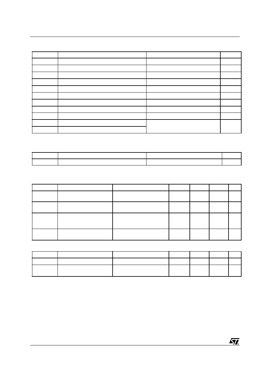
Figure 1: Package
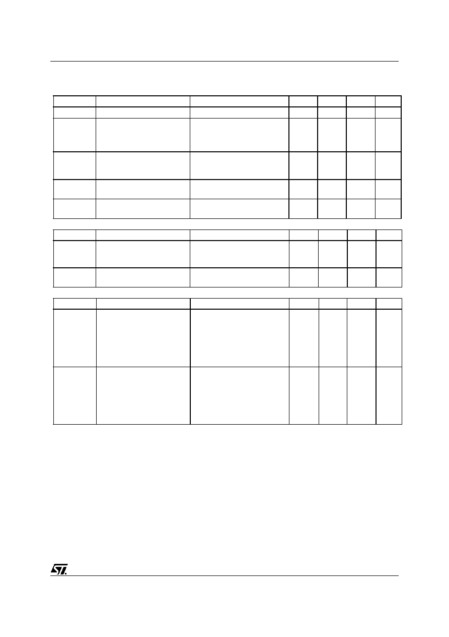
Figure 2: Internal Schematic Diagram
TYPE
V
CES
V
CE(sat)
(Max)
@25∞C
I
C
@100∞C
STGF7NB60SL
200 V
< 0.045
40 A
1
2
3
SALES TYPE
MARKING
PACKAGE
PACKAGING
STGF7NB60SL
GF7NB60SL
TO-220FP
TUBE
Rev. 2
STGF7NB60SL
2/9
Table 3: Absolute Maximum ratings
(1)Pulse width limited by max. junction temperature.
Table 4: Thermal Data
ELECTRICAL CHARACTERISTICS (T
CASE
=25∞C UNLESS OTHERWISE SPECIFIED)
Table 5: Off
Table 6: On
Symbol
Parameter
Value
Symbol
V
CES
Collector-Emitter Voltage (V
GS
= 0)
600
V
V
ECR
Reverse Battery Protection
20
V
V
GE
Gate-Emitter Voltage
± 20
V
I
C
Collector Current (continuous) at 25∞C
15
A
I
C
Collector Current (continuous) at 100∞C
7
A
I
CM
(1)
Collector Current (pulsed)
20
A
P
TOT
Total Dissipation at T
C
= 25∞C
25
W
Derating Factor
0.2
W/∞C
V
ISO
Insulation Withstand Voltage A.C.
2500
V
T
stg
Storage Temperature
≠ 55 to 150
∞C
T
j
Operating Junction Temperature
Rthj-case
Thermal Resistance Junction-case Max
5
∞C/W
Rthj-amb
Thermal Resistance Junction-ambient Max
62.5
∞C/W
Symbol
Parameter
Test Conditions
Min.
Typ.
Max.
Unit
V
BR(CES)
Collectro-Emitter Breakdown
Voltage
I
C
= 250 µA, V
GE
= 0
600
V
V
BR(ECS)
Emitter-Collector Breakdown
Voltage
I
C
= 1mA, V
GE
= 0
20
V
I
CES
Collector-Emitter Leakage
Current (V
CE
= 0)
V
GE
= Max Rating
Tc=25∞C
Tc=125∞C
10
100
µA
µA
I
GES
Gate-Emitter Leakage
Current (V
CE
= 0)
V
GE
= ± 20 V , V
CE
= 0
±100
nA
Symbol
Parameter
Test Conditions
Min.
Typ.
Max.
Unit
V
GE(th)
Gate Threshold Voltage
V
CE
= V
GE
, I
C
= 250 µA
1.2
2.4
V
V
CE(SAT)
Collector-Emitter Saturation
Voltage
V
GE
=4.5 V, I
C
= 7A, Tj= 25∞C
V
GE
=4.5 V, I
C
= 7A, Tj= 125∞C
1.2
1.1
1.6
V
V
3/9
STGF7NB60SL
ELECTRICAL CHARACTERISTICS (CONTINUED)
Table 7: Dynamic
Table 8: Switching On
Table 9: Switching Off
(**)Turn-off losses include also the tail of the collector current.
Symbol
Parameter
Test Conditions
Min.
Typ.
Max.
Unit
g
fs
Forward Transconductance
V
CE
= 15 V
,
I
C
= 7 A
5
S
C
ies
C
oes
C
res
Input Capacitance
Output Capacitance
Reverse Transfer
Capacitance
V
CE
= 25V, f = 1 MHz, V
GE
= 0
800
60
10
pF
pF
pF
Q
g
Q
ge
Q
gc
Total Gate Charge
Gate-Emitter Charge
Gate-Collector Charge
V
CE
= 480V, I
C
= 7 A,
V
GE
= 5V
(see Figure 20)
16
2.5
8.5
22
nC
nC
nC
I
CL
Turn-Off SOA Minimum
Current
V
clamp
= 480 V
,
Tj = 125∞C
R
G
= 1 K
,
V
GE
=5V
20
A
tscw
Short Circuit Withstand Time
V
ce
= 0.5 V
BR(CES)
, V
GE
=5V
,
Tj = 125∞C , R
G
= 1K
14
µs
Symbol
Parameter
Test Conditions
Min.
Typ.
Max.
Unit
t
d(on)
t
r
Turn-on Delay Time
Current Rise Time
V
CC
= 480 V, I
C
= 7 A R
G
=1K
,
V
GE
= 5 V
(see Figure 18)
1.1
0.25
µs
µs
(di/dt)
on
E
on
Turn-on Current Slope
Turn-on Switching Losses
V
CC
= 480 V, I
C
= 7 A R
G
=1K
V
GE
= 5 V,Tj = 125∞C
45
2.7
A/µs
mJ
Symbol
Parameter
Test Conditions
Min.
Typ.
Max.
Unit
t
c
Cross-over Time
V
cc
= 480 V, I
C
= 7 A,
R
GE
= 1K
, V
GE
= 5 V
(see Figure 18)
2.7
µs
t
r
(V
off
)
Off Voltage Rise Time
1.6
µs
t
d
(
off
)
Delay Time
5.2
µs
t
f
Current Fall Time
1.1
µs
E
off
(**)
Turn-off Switching Loss
4.1
m
J
t
c
Cross-over Time
V
cc
= 480 V, I
C
= 7 A,
R
GE
= 1K
, V
GE
= 5 V
Tj = 125 ∞C
(see Figure 18)
4.4
µs
t
r
(V
off
)
Off Voltage Rise Time
2.4
µs
t
d
(
off
)
Delay Time
6.4
µs
t
f
Fall Time
1.7
µs
E
off
(**)
Turn-off Switching Loss
7.1
m
J

STGF7NB60SL
4/9
Figure 3: Output Characteristics
Figure 4: Transconductance
Figure 5: Collector-Emitter On Voltage vs Col-
lector Current
Figure 6: Transfer Characteristics
Figure 7: Collector-Emitter On Voltage vs Tem-
perature
Figure 8: Normalized Collector-Emitter On
Voltage vs Temperature
5/9
STGF7NB60SL
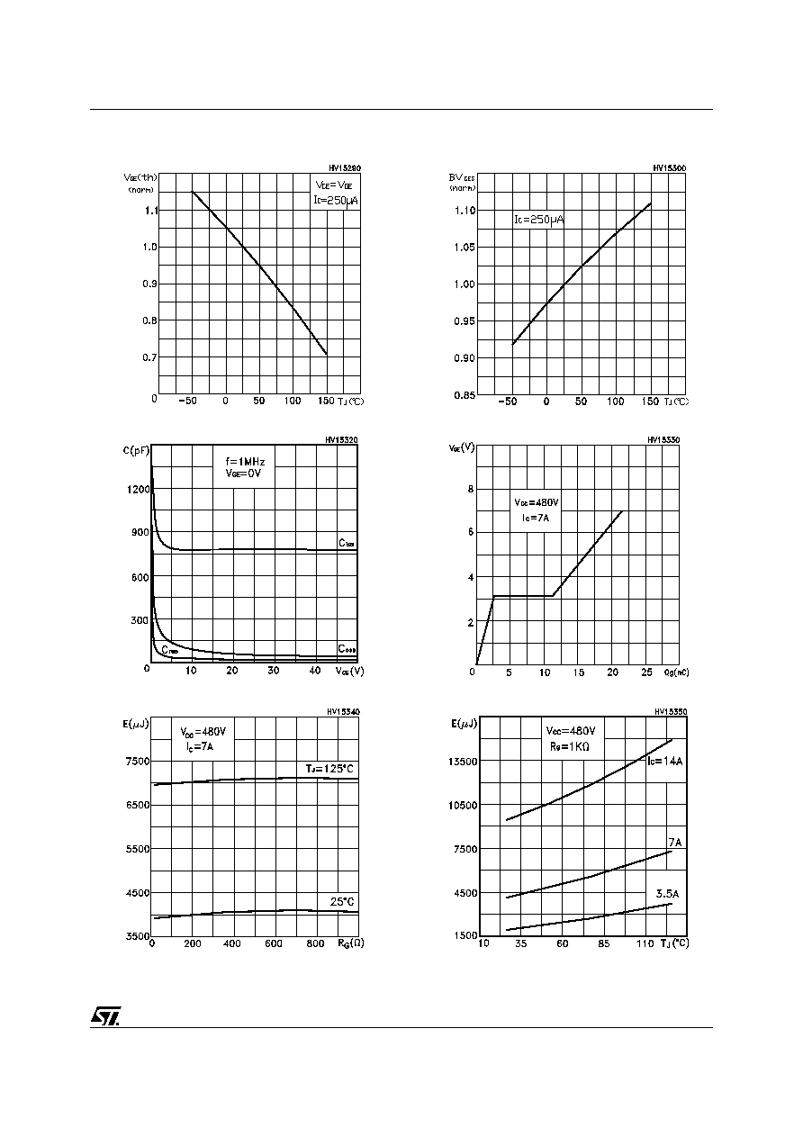
Figure 9: Gate Thereshold vs Temperature
Figure 10: Capacitance Variations
Figure 11: Total Switching Losses vs Gate Re-
sistance
Figure 12: Normalized Breakdown Voltage vs
Temperature
Figure 13: Gate Charge vs Gate-Emitter Volt-
age
Figure 14: Total Switching Losses vs Temper-
ature