1/8
June 2002
STGP10NB60SFP
N-CHANNEL 10A - 600V - TO-220FP
PowerMeshTM IGBT
(
q
) Pulse width limited by safe operating area
s
HIGHT INPUT IMPEDANCE (VOLTAGE
DRIVEN)
s
LOW ON-VOLTAGE DROP
s
HIGH CURRENT CAPABILITY
s
OFF LOSSES INCLUDE TAIL CURRENT
DESCRIPTION
Using the latest high voltage technology based on a
patented strip layout, STMicroelectronics has
designed an advanced family of IGBTs, the
PowerMESH
TM
IGBTs, with outstanding
performances. The suffix "S" identifies a family
optimized achieve minimum on-voltage drop for low
frequency applications (<1kHz).
APPLICATIONS
s
LIGHT DIMMER
s
STATIC RELAYS
s
MOTOR CONTROL
ABSOLUTE MAXIMUM RATINGS
TYPE
V
CES
V
CE(sat)
I
C
STGP10NB60SFP
600
< 1.7
V
10 A
Symbol
Parameter
Value
Unit
V
CES
Collector-Emitter Voltage (V
GS
= 0)
600
V
V
ECR
Reverse Battery Protection
20
V
V
GE
Gate-Emitter Voltage
± 20
V
I
C
Collector Current (continuous) at T
C
= 25∞C
20
A
I
C
Collector Current (continuous) at T
C
= 100∞C
10
A
I
CM
(
n
)
Collector Current (pulsed)
80
A
P
TOT
Total Dissipation at T
C
= 25∞C
31.5
W
Derating Factor
0.21
W/∞C
T
stg
Storage Temperature
≠65 to 150
∞C
T
j
Max. Operating Junction Temperature
150
∞C
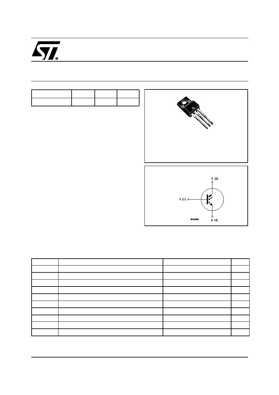
TO-220FP
1
2
3
INTERNAL SCHEMATIC DIAGRAM

STGP10NB60SFP
2/8
THERMAL DATA
ELECTRICAL CHARACTERISTICS (TCASE = 25 ∞C UNLESS OTHERWISE SPECIFIED)
OFF
ON
(1)
DYNAMIC
Rthj-case
Thermal Resistance Junction-case Max
4.7
∞C/W
Rthj-amb
Thermal Resistance Junction-ambient Max
62.5
∞C/W
Rthc-sink
Thermal Resistance Case-sink Typ
0.5
∞C/W
Symbol
Parameter
Test Conditions
Min.
Typ.
Max.
Unit
V
BR(CES)
Collector-Emitter Break-down
Voltage
I
C
= 250 µA, V
GE
= 0,
600
V
V
BR(CES)
Emitter Collector Break-down
Voltage
I
C
= 1 mA, V
GE
= 0,
20
V
I
CES
Collector cut-off Current
(V
GE
= 0)
V
CE
= Max Rating ,T
j
=25 ∞C
V
CE
= Max Rating ,T
j
=125 ∞C
10
100
µA
µA
I
GES
Gate-Emitter Leakage
Current (V
CE
= 0)
V
GE
= ± 20V , V
CE
= 0
± 100
nA
Symbol
Parameter
Test Conditions
Min.
Typ.
Max.
Unit
V
GE(th)
Gate Threshold Voltage
V
CE
= V
GE
, I
C
= 250µA
2.5
5
V
V
CE(SAT)
Collector-Emitter Saturation
Voltage
V
GE
=15V, I
C
= 5 A, Tj= 25∞C
V
GE
=15V, I
C
= 10 A, Tj= 25∞C
V
GE
=15V, I
C
= 10 A, Tj= 125∞C
1.15
1.35
1.25
1.7
V
V
V
Symbol
Parameter
Test Conditions
Min.
Typ.
Max.
Unit
g
fs
Forward Transconductance
V
CE
= 25 V
,
I
C
=10 A
5
S
C
ies
Input Capacitance
V
CE
= 25V, f = 1 MHz, V
GE
= 0
610
pF
C
oes
Output Capacitance
65
pF
C
res
Reverse Transfer
Capacitance
12
pF
Q
g
Gate Charge
V
CE
= 400V, I
C
= 10 A,
V
GE
= 15V
33
nC
I
CL
Latching Current
V
clamp
= 480V, RG= 1k
,
Tj= 125∞C
20
A
3/8
STGP10NB60SFP
SWITCHING ON
SWITCHING OFF
(
q
)Pulsed: Pulse duration = 300
µ
s, duty cycle 1.5 %.
(1)Pulse width limited by max. junction temperature.
(**)Losses Include Also the Tail
Symbol
Parameter
Test Conditions
Min.
Typ.
Max.
Unit
t
d(on)
Turn-on Delay Time
V
CC
= 480 V, I
C
= 10 A
R
G
= 1K
, V
GE
= 15 V
0.7
µs
t
r
Rise Time
0.46
µs
(di/dt)
on
Eon
Turn-on Current Slope
Turn-on Switching Losses
V
CC
= 480 V, I
C
= 10 A
R
G
=1K
, V
GE
= 15 V
8
0.6
A/µs
mJ
Symbol
Parameter
Test Conditions
Min.
Typ.
Max.
Unit
t
c
Cross-over Time
V
clamp
= 480 V, I
C
= 10 A,
R
GE
= 1K
, V
GE
= 15 V
2.2
µs
t
r
(V
off
)
Off Voltage Rise Time
1.2
µs
t
f
Fall Time
1.2
µs
E
off
(**)
Turn-off Switching Loss
5.0
mJ
t
c
Cross-over Time
V
clamp
= 480 V, I
C
= 10 A,
R
GE
= 1K
, V
GE
= 15 V
Tj = 125 ∞C
3.8
µs
t
r
(V
off
)
Off Voltage Rise Time
1.2
µs
t
f
Fall Time
1.9
µs
E
off
(**)
Turn-off Switching Loss
8.0
mJ
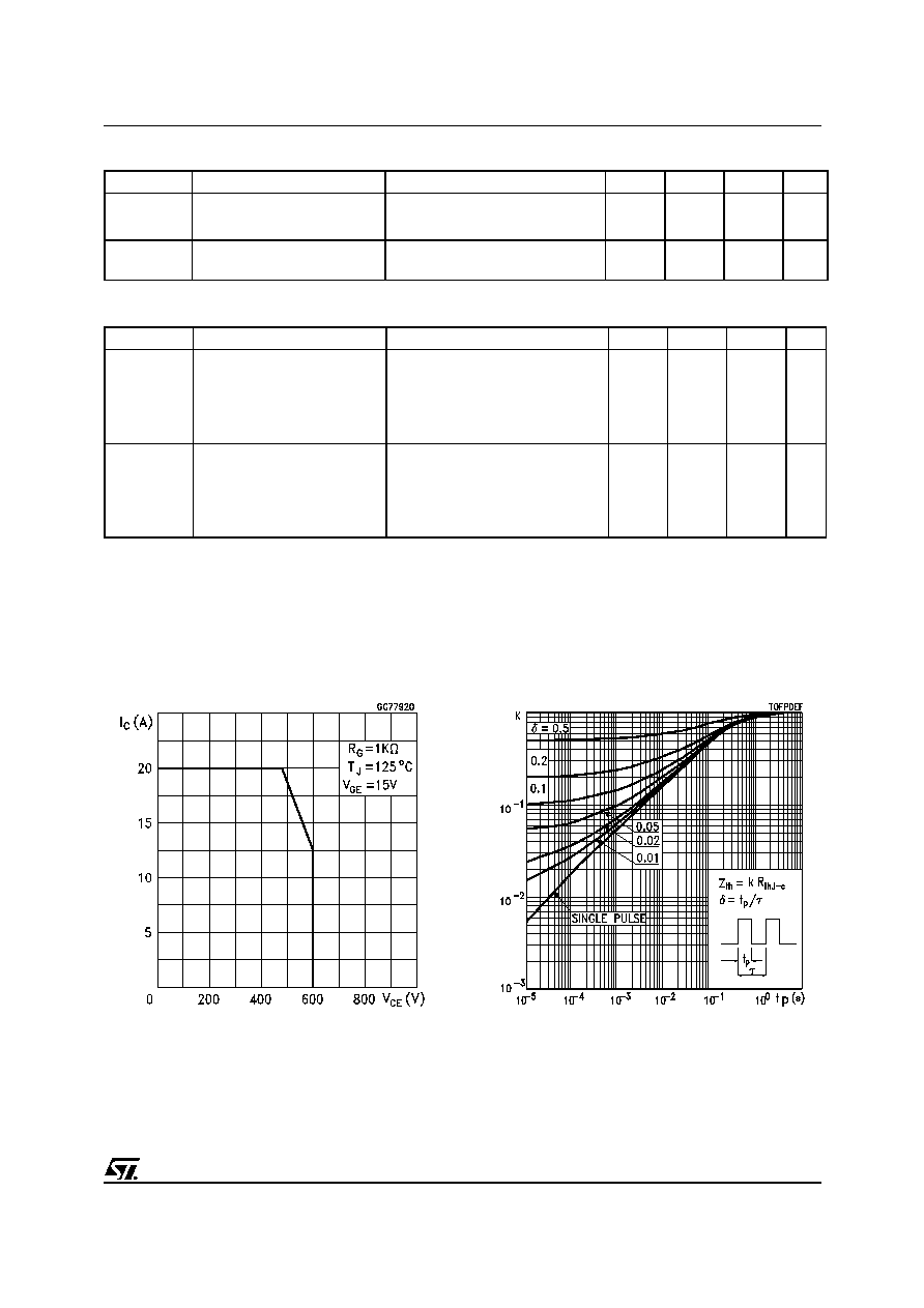
Thermal Impedance
Switching Off Safe Operating Area
STGP10NB60SFP
4/8
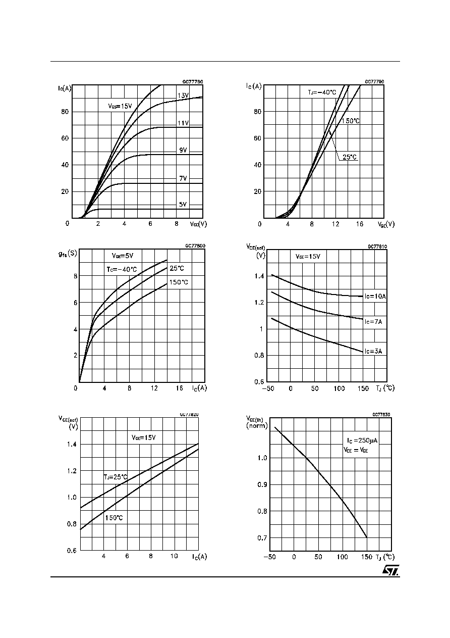
Gate Threshold Voltage vs Temperature
Transconductance
Transfer Characteristics
Output Characteristics
Collector-Emitter On Voltage vs Temperature
Collector-Emitter On Voltage vs Collector Cur-
rent
5/8
STGP10NB60SFP
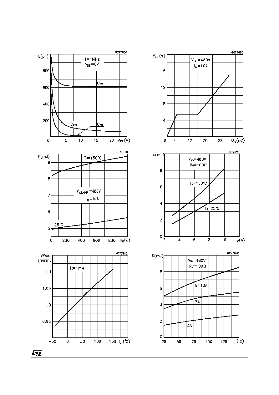
Off Losses vs Gate Resistance
Off Losses vs Collector Current
Gate Charge vs Gate-Emitter Voltage
Capacitance Variations
Normalized Break-down Voltage vs Temp.
Off Losses vs Temperature