1/14
July 2005
STGP14NC60KD - STGF14NC60KD
STGB14NC60KD
N-CHANNEL 14A - 600V - TO-220/TO-220FP/D
2
PAK
SHORT CIRCUIT RATED PowerMESHTM IGBT
Table 1: General Features
LOWER ON-VOLTAGE DROP (V
cesat
)
OFF LOSSES INCLUDE TAIL CURRENT
LOWER C
RES
/ C
IES
RATIO
SWITCHING LOSSES INCLUDE DIODE
RECOVERY ENERGY
VERY SOFT ULTRA FAST RECOVERY
ANTIPARALLEL DIODE
NEW GENERATION PRODUCTS WITH
TIGHTER PARAMETER DISTRUBUTION
DESCRIPTION
Using the latest high voltage technology based on
a patented strip layout, STMicroelectronics has
designed an advanced family of IGBTs, the Pow-
erMESH
TM
IGBTs, with outstanding performances.
The suffix "K" identifies a family optimized for high
frequency motor control applications with short cir-
cuit withstand capability.
APPLICATIONS
HIGH FREQUENCY INVERTERS
SMPS and PFC IN BOTH HARD SWITCH AND
RESONANT TOPOLOGIES
MOTOR DRIVERS
Table 2: Order Codes
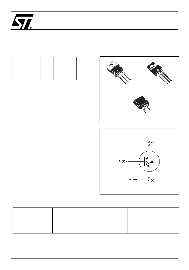
Figure 1: Package
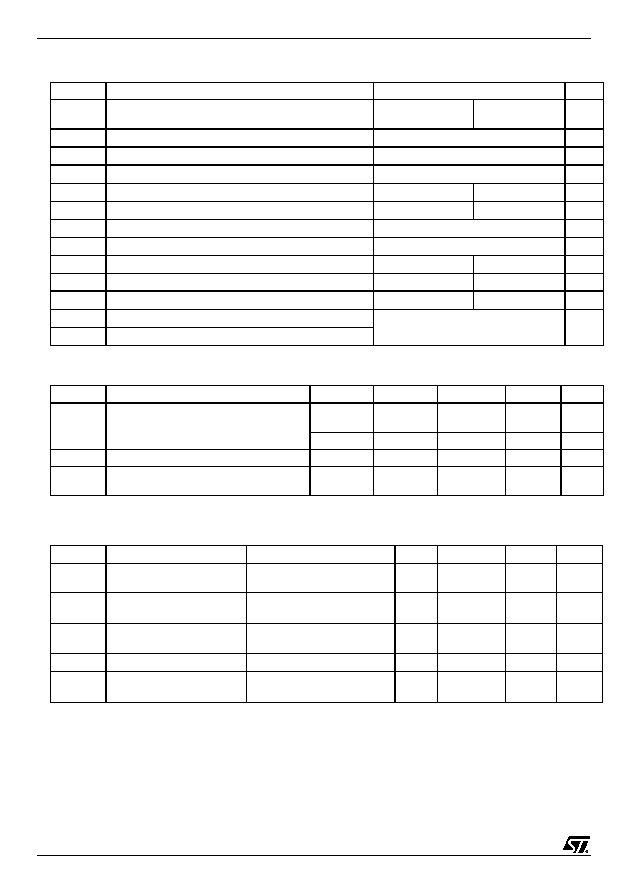
Figure 2: Internal Schematic Diagram
TYPE
V
CES
V
CE(sat)
(Max)
@25∞C
I
C
(#)
@100∞C
STGB14NC60KD
STGF14NC60KD
STGP14NC60KD
600 V
600 V
600 V
< 2.5 V
< 2.5 V
< 2.5 V
14 A
7 A
14 A
TO-220
1
2
3
1
2
3
1
3
TO-220FP
D
2
PAK
SALES TYPE
MARKING
PACKAGE
PACKAGING
STGB14NC60KDT4
GB14NC60KD
D
2
PAK
TAPE & REEL
STGF14NC60KD
GF14NC60KD
TO-220FP
TUBE
STGP14NC60KD
GP14NC60KD
TO-220
TUBE
Rev.2
STGP14NC60KD - STGF14NC60KD - STGB14NC60KD
2/14
Table 3: Absolute Maximum ratings
( ) Pulse width limited by Max Junction Temperature.
Table 4: Thermal Data
ELECTRICAL CHARACTERISTICS (T
CASE
=25∞C UNLESS OTHERWISE SPECIFIED)
Table 5: Main Parameters
(#) Calculated according to the iterative formula:
Symbol
Parameter
Value
Unit
STGB14NC60KD
STGP14NC60KD
STGF14NC60KD
V
CES
Collector-Emitter Voltage (V
GS
= 0)
600
V
V
ECR
Emitter-Collector Voltage
20
V
V
GE
Gate-Emitter Voltage
±20
V
I
C
Collector Current (continuous) at T
C
= 25∞C (#)
25
11
A
I
C
Collector Current (continuous) at T
C
= 100∞C (#)
14
7
A
I
CM
( )
Collector Current (pulsed)
50
A
I
F
Diode RMS Forward Current at T
C
= 25∞C
20
A
P
TOT
Total Dissipation at T
C
= 25∞C
80
25
W
Derating Factor
0.64
0.20
W/∞C
V
ISO
Insulation Withstand Voltage A.C.(t = 1 sec; Tc = 25∞C)
--
2500
V
T
stg
Storage Temperature
≠ 55 to 150
∞C
T
j
Operating Junction Temperature
Min.
Typ.
Max.
Rthj-case
Thermal Resistance Junction-case
TO-220
D≤PAK
1.56
∞C/W
TO-220FP
5.0
∞C/W
Rthj-amb
Thermal Resistance Junction-ambient
62.5
∞C/W
T
L
Maximum Lead Temperature for Soldering
Purpose (1.6 mm from case, for 10 sec.)
300
∞C
Symbol
Parameter
Test Conditions
Min.
Typ.
Max.
Unit
V
BR(CES)
Collector-Emitter
Breakdown Voltage
I
C
= 1 mA, V
GE
= 0
600
V
I
CES
Collector cut-off Current
(V
GE
= 0)
V
CE
= Max Rating, T
C
= 25∞C
V
CE
= Max Rating, T
C
= 125∞C
10
1
µA
mA
I
GES
Gate-Emitter Leakage
Current (V
CE
= 0)
V
GE
= ±20V , V
CE
= 0
±100
nA
V
GE(th)
Gate Threshold Voltage
V
CE
= V
GE
, I
C
= 250 µA
5
7
V
V
CE(sat)
Collector-Emitter Saturation
Voltage
V
GE
= 15V, I
C
= 7A
V
GE
= 15V, I
C
= 7A, Tc= 125∞C
2.0
1.8
2.5
V
V
I
C
T
C
(
)
T
JMAX
T
C
≠
R
THJ
C
≠
V
C ESAT MAX
(
)
T
C
I
C
,
(
)
◊
--------------------------------------------------------------------------------------------------
=
3/14
STGP14NC60KD - STGF14NC60KD - STGB14NC60KD
ELECTRICAL CHARACTERISTICS (CONTINUED)
Table 6: Dynamic
Table 7: Switching On
Table 8: Switching Off
Table 9: Switching Energy
(1) Pulsed: Pulse duration = 300 µs, duty cycle 1.5%
(2) Eon is the turn-on losses when a typical diode is used in the test circuit in figure 2. If the IGBT is offered in a package with a co-pack diode,
the co-pack diode is used as external diode. IGBTs & DIODE are at the same temperature (25∞C and 125∞C)
(3)Turn-off losses include also the tail of the collector current.
Symbol
Parameter
Test Conditions
Min.
Typ.
Max.
Unit
g
fs
(1)
Forward Transconductance
V
CE
= 15 V
,
I
C
= 7 A
3
S
C
ies
Input Capacitance
V
CE
= 25 V, f= 1 MHz, V
GE
= 0
760
pF
C
oes
Output Capacitance
86
pF
C
res
Reverse Transfer
Capacitance
15.5
pF
Q
g
Q
ge
Q
gc
Total Gate Charge
Gate-Emitter Charge
Gate-Collector Charge
V
CE
= 390 V, I
C
= 7 A,
V
GE
= 15 V
(see Figure 21)
34.4
8.1
16.4
nC
nC
nC
t
scw
Short Circuit Withstand Time
V
CE
= 0.5 V
BR(CES)
,T
j
= 125∞C,
R
G
= 10
,
V
GE
= 12 V
10
µs
Symbol
Parameter
Test Conditions
Min.
Typ.
Max.
Unit
t
d(on)
t
r
(di/dt)
on
Turn-on Delay Time
Current Rise Time
Turn-on Current Slope
V
CC
= 390 V, I
C
= 7 A
R
G
= 10
, V
GE
= 15V, Tj= 25∞C
(see Figure 19)
22.5
8.5
700
ns
ns
A/µs
t
d(on)
t
r
(di/dt)
on
Turn-on Delay Time
Current Rise Time
Turn-on Current Slope
V
CC
= 390 V, I
C
= 7 A
R
G
= 10
, V
GE
= 15V, Tj= 125∞C
(see Figure 19)
22
9.5
680
ns
ns
A/µs
Symbol
Parameter
Test Conditions
Min.
Typ.
Max.
Unit
t
r
(V
off
)
t
d
(
off
)
t
f
Off Voltage Rise Time
Turn-off Delay Time
Current Fall Time
V
cc
= 390 V, I
C
= 7 A,
R
GE
= 10
, V
GE
= 15 V
T
J
= 25 ∞C
(see Figure 19)
60
116
75
ns
ns
ns
t
r
(V
off
)
t
d
(
off
)
t
f
Off Voltage Rise Time
Turn-off Delay Time
Current Fall Time
V
cc
= 390 V, I
C
= 7 A,
R
GE
= 10
, V
GE
= 15 V
Tj = 125 ∞C
(see Figure 19)
24
196
144
ns
ns
ns
Symbol
Parameter
Test Conditions
Min.
Typ.
Max.
Unit
Eon
(2)
E
off
(3)
E
ts
Turn-on Switching Losses
Turn-off Switching Losses
Total Switching Losses
V
CC
= 390 V, I
C
= 7 A
R
G
= 10
, V
GE
= 15V, Tj= 25∞C
(see Figure 19)
82
155
237
µJ
µJ
µJ
Eon
(2)
E
off
(3)
E
ts
Turn-on Switching Losses
Turn-off Switching Losses
Total Switching Losses
V
CC
= 390 V, I
C
= 7 A
R
G
= 10
, V
GE
= 15V, Tj= 125∞C
(see Figure 19)
131
370
501
µJ
µJ
µJ
STGP14NC60KD - STGF14NC60KD - STGB14NC60KD
4/14
Table 10: Collector-Emitter Diode
Symbol
Parameter
Test Condiction
Min.
Typ.
Max.
Unit
V
f
Forward On-Voltage
If = 3.5 A
If = 3.5 A, Tj = 125 ∞C
1.3
1.1
1.9
V
V
t
rr
t
a
Q
rr
I
rrm
S
Reverse Recovery Time
Reverse Recovery Charge
Reverse Recovery Current
Softness factor of the diode
If = 7 A, V
R
= 40 V,
T
j
= 25 ∞C, di/dt = 100 A/µs
37
22
40
2.1
0.68
ns
ns
nC
A
t
rr
t
a
Q
rr
I
rrm
S
Reverse Recovery Time
Reverse Recovery Charge
Reverse Recovery Current
Softness factor of the diode
If = 7 A, V
R
= 40 V,
T
j
= 125 ∞C, di/dt = 100 A/µs
61
34
98
3.2
0.79
ns
ns
nC
A
5/14
STGP14NC60KD - STGF14NC60KD - STGB14NC60KD
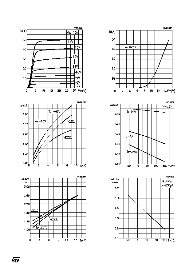
Figure 3: Output Characteristics
Figure 4: Transconductance
Figure 5: Collector-Emitter On Voltage vs Col-
lector Current
Figure 6: Transfer Characteristics
Figure 7: Collector-Emitter On Voltage vs Tem-
perature
Figure 8: Normalized Gate Threshold vs Tem-
perature
STGP14NC60KD - STGF14NC60KD - STGB14NC60KD
6/14
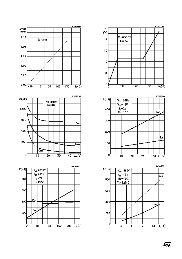
Figure 9: Normalized Breakdown Voltage vs
Temperature
Figure 10: Capacitance Variations
Figure 11: Total Switching Losses vs Gate Re-
sistance
Figure 12: Gate Charge vs Gate-Emitter Volt-
age
Figure 13: Total Switching Losses vs Temper-
ature
Figure 14: Total Switching Losses vs Collector
Current
7/14
STGP14NC60KD - STGF14NC60KD - STGB14NC60KD
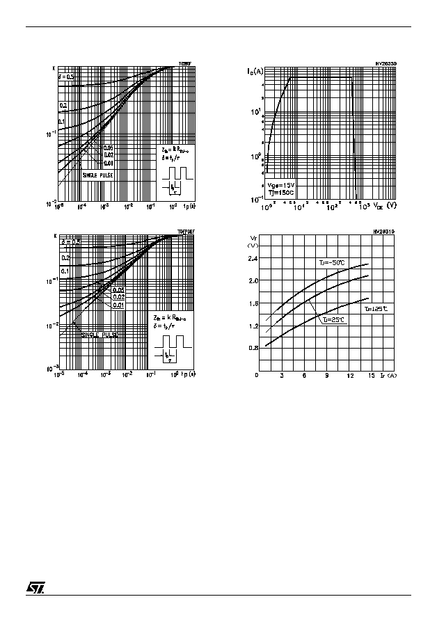
Figure 15: Thermal Impedance For TO-220/
D≤PAK
Figure 16: Thermal Impedance For TO-220FP
Figure 17: Turn-Off SOA
Figure 18: Emitter-Collector Diode
Characteristics
STGP14NC60KD - STGF14NC60KD - STGB14NC60KD
8/14
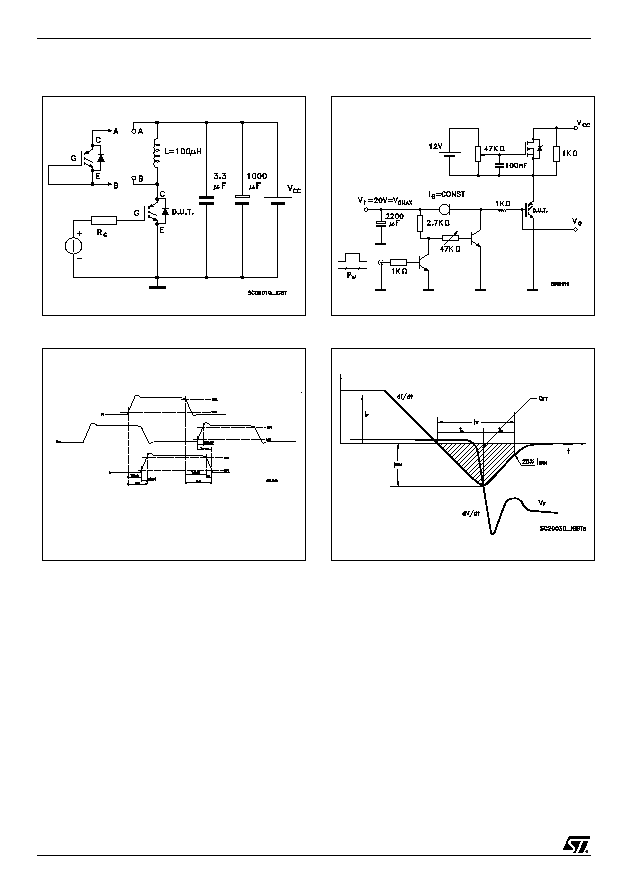
Figure 19: Test Circuit for Inductive Load
Switching
Figure 20: Switching Waveforms
Figure 21: Gate Charge Test Circuit
Figure 22: Diode Recovery Times Waveform
9/14
STGP14NC60KD - STGF14NC60KD - STGB14NC60KD
TO-247 MECHANICAL DATA
1
DIM.
mm.
inch
MIN.
TYP
MAX.
MIN.
TYP.
MAX.
A
4.4
4.6
0.173
0.181
A1
2.49
2.69
0.098
0.106
A2
0.03
0.23
0.001
0.009
B
0.7
0.93
0.027
0.036
B2
1.14
1.7
0.044
0.067
C
0.45
0.6
0.017
0.023
C2
1.23
1.36
0.048
0.053
D
8.95
9.35
0.352
0.368
D1
8
0.315
E
10
10.4
0.393
E1
8.5
0.334
G
4.88
5.28
0.192
0.208
L
15
15.85
0.590
0.625
L2
1.27
1.4
0.050
0.055
L3
1.4
1.75
0.055
0.068
M
2.4
3.2
0.094
0.126
R
0.4
0.015
V2
0∫
4∫
D
2
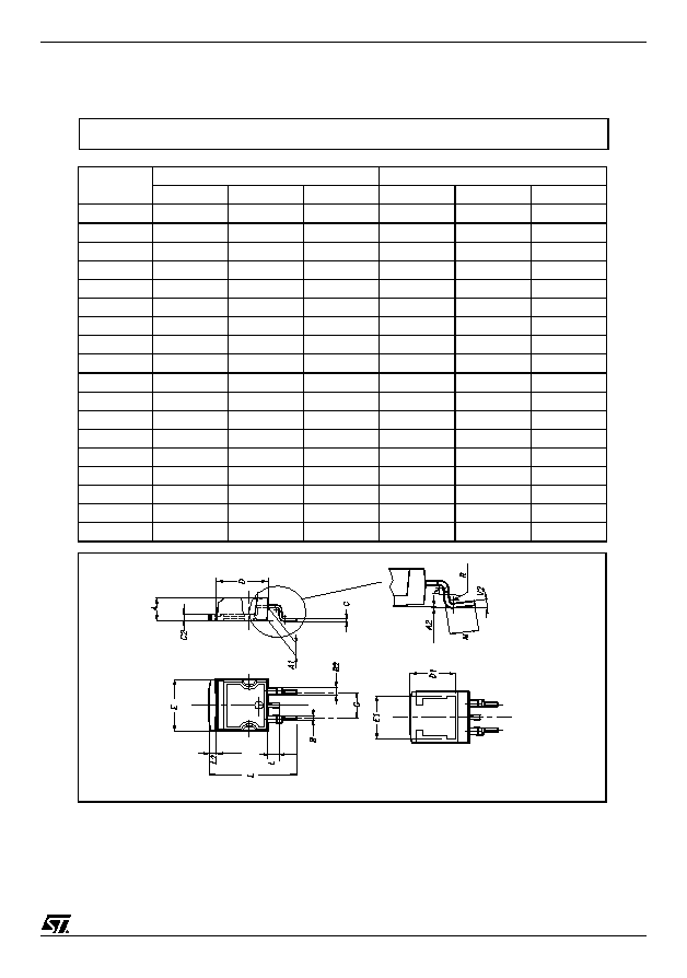
PAK MECHANICAL DATA
3
STGP14NC60KD - STGF14NC60KD - STGB14NC60KD
10/14
L2
A
B
D
E
H
G
L6
F
L3
G1
1 2 3
F2
F1
L7
L4
L5
DIM.
mm.
inch
MIN.
TYP
MAX.
MIN.
TYP.
MAX.
A
4.4
4.6
0.173
0.181
B
2.5
2.7
0.098
0.106
D
2.5
2.75
0.098
0.108
E
0.45
0.7
0.017
0.027
F
0.75
1
0.030
0.039
F1
1.15
1.7
0.045
0.067
F2
1.15
1.7
0.045
0.067
G
4.95
5.2
0.195
0.204
G1
2.4
2.7
0.094
0.106
H
10
10.4
0.393
0.409
L2
16
0.630
L3
28.6
30.6
1.126
1.204
L4
9.8
10.6
.0385
0.417
L5
2.9
3.6
0.114
0.141
L6
15.9
16.4
0.626
0.645
L7
9
9.3
0.354
0.366
ÿ
3
3.2
0.118
0.126
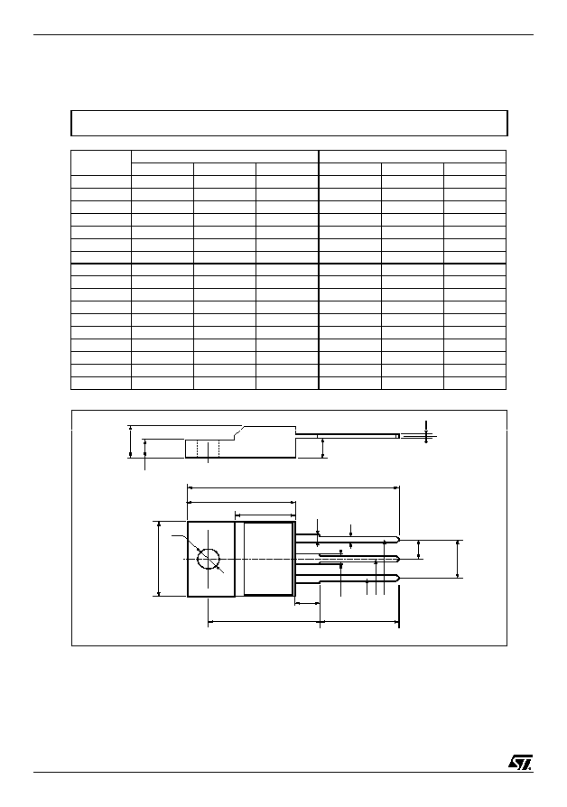
TO-220FP MECHANICAL DATA
11/14
STGP14NC60KD - STGF14NC60KD - STGB14NC60KD
DIM.
mm.
inch
MIN.
TYP
MAX.
MIN.
TYP.
MAX.
A
4.40
4.60
0.173
0.181
b
0.61
0.88
0.024
0.034
b1
1.15
1.70
0.045
0.066
c
0.49
0.70
0.019
0.027
D
15.25
15.75
0.60
0.620
E
10
10.40
0.393
0.409
e
2.40
2.70
0.094
0.106
e1
4.95
5.15
0.194
0.202
F
1.23
1.32
0.048
0.052
H1
6.20
6.60
0.244
0.256
J1
2.40
2.72
0.094
0.107
L
13
14
0.511
0.551
L1
3.50
3.93
0.137
0.154
L20
16.40
0.645
L30
28.90
1.137
¯P
3.75
3.85
0.147
0.151
Q
2.65
2.95
0.104
0.116
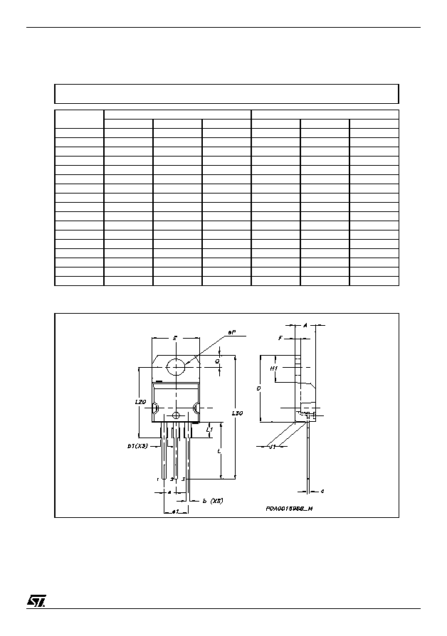
TO-220 MECHANICAL DATA
STGP14NC60KD - STGF14NC60KD - STGB14NC60KD
12/14
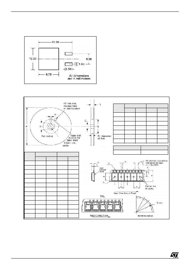
TAPE AND REEL SHIPMENT
D
2
PAK FOOTPRINT
* on sales type
DIM.
mm
inch
MIN.
MAX.
MIN.
MAX.
A
330
12.992
B
1.5
0.059
C
12.8
13.2
0.504
0.520
D
20.2
0795
G
24.4
26.4
0.960
1.039
N
100
3.937
T
30.4
1.197
BASE QTY
BULK QTY
1000
1000
REEL MECHANICAL DATA
DIM.
mm
inch
MIN.
MAX.
MIN.
MAX.
A0
10.5
10.7
0.413
0.421
B0
15.7
15.9
0.618
0.626
D
1.5
1.6
0.059
0.063
D1
1.59
1.61
0.062
0.063
E
1.65
1.85
0.065
0.073
F
11.4
11.6
0.449
0.456
K0
4.8
5.0
0.189
0.197
P0
3.9
4.1
0.153
0.161
P1
11.9
12.1
0.468
0.476
P2
1.9
2.1
0.075
0.082
R
50
1.574
T
0.25
0.35
0.0098 0.0137
W
23.7
24.3
0.933
0.956
TAPE MECHANICAL DATA
13/14
STGP14NC60KD - STGF14NC60KD - STGB14NC60KD
Table 11: Revision History
Date
Revision
Description of Changes
14-Jun-2005
1
New release
22-Jul-2005
2
Complete version

STGP14NC60KD - STGF14NC60KD - STGB14NC60KD
14/14
Information furnished is believed to be accurate and reliable. However, STMicroelectronics assumes no responsibility for the consequences
of use of such information nor for any infringement of patents or other rights of third parties which may result from its use. No license is granted
by implication or otherwise under any patent or patent rights of STMicroelectronics. Specifications mentioned in this publication are subject
to change without notice. This publication supersedes and replaces all information previously supplied. STMicroelectronics products are not
authorized for use as critical components in life support devices or systems without express written approval of STMicroelectronics.
The ST logo is a registered trademark of STMicroelectronics
All other names are the property of their respective owners
© 2005 STMicroelectronics - All Rights Reserved
STMicroelectronics group of companies
Australia - Belgium - Brazil - Canada - China - Czech Republic - Finland - France - Germany - Hong Kong - India - Israel - Italy - Japan -
Malaysia - Malta - Morocco - Singapore - Spain - Sweden - Switzerland - United Kingdom - United States of America
www.st.com