 | –≠–ª–µ–∫—Ç—Ä–æ–Ω–Ω—ã–π –∫–æ–º–ø–æ–Ω–µ–Ω—Ç: STGP7NB60 | –°–∫–∞—á–∞—Ç—å:  PDF PDF  ZIP ZIP |
STGP7NB60H
N-CHANNEL 7A - 600V TO-220
PowerMESH
TM
IGBT
s
HIGH INPUT IMPEDANCE
(VOLTAGE DRIVEN)
s
LOW ON-VOLTAGE DROP (V
cesat
)
s
LOW GATE CHARGE
s
HIGH CURRENT CAPABILITY
s
VERY HIGH FREQUENCY OPERATION
s
OFF LOSSES INCLUDE TAIL CURRENT
DESCRIPTION
Using the latest high voltage technology based
on a patented strip layout, STMicroelectronics
has designed an advanced family of IGBTs, the
PowerMESH
TM
IGBTs,
with
outstanding
perfomances. The suffix "H" identifies a family
optimized to achieve very low switching times for
high frequency applications (<120kHz).
APPLICATIONS
s
HIGH FREQUENCY MOTOR CONTROLS
s
SMPS AND PFC IN BOTH HARD SWITCH
AND RESONANT TOPOLOGIES
Æ
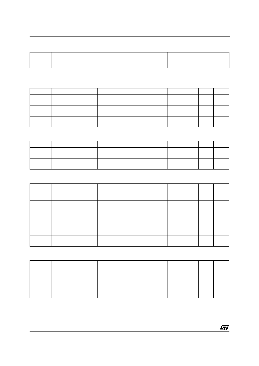
INTERNAL SCHEMATIC DIAGRAM
ABSOLUTE MAXIMUM RATINGS
Symbol
Parameter
Value
Unit
V
CES
Collector-Emitter Volt age (V
G S
= 0)
600
V
V
ECR
Emitter-Collector Volt age
20
V
V
GE
G ate-Emitter Voltage
±
20
V
I
C
Collector Current (continuous) at T
c
= 25
o
C
14
A
I
C
Collector Current (continuous) at T
c
= 100
o
C
7
A
I
CM
(
∑
)
Collector Current (pulsed)
56
A
P
tot
T otal Dissipation at T
c
= 25
o
C
80
W
Derating Fact or
0. 64
W /
o
C
T
s tg
Storage T emperature
-65 t o 150
o
C
T
j
Max. Operating Junction Temperat ure
150
o
C
(
∑
) Pulse width limited by safe operating area
TYPE
V
CES
V
CE(sat )
I
C
STGP7NB60H
600 V
< 2.8 V
7 A
June 1999
1
2
3
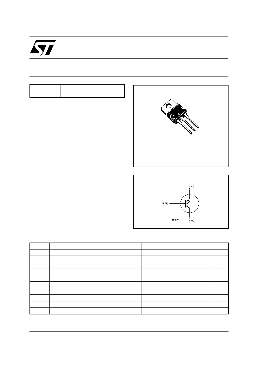
TO-220
1/8
THERMAL DATA
R
thj -case
R
thj -amb
R
thc-sink
Thermal Resistance Junction-case
Max
Thermal Resistance Junction-ambient
Max
Thermal Resistance Case-sink
T yp
1.56
62. 5
0.5
o
C/W
o
C/W
o
C/W
ELECTRICAL CHARACTERISTICS (T
j
= 25
o
C unless otherwise specified)
OFF
Symbol
Parameter
Test Conditions
Min.
Typ.
Max.
Unit
V
BR(CES)
Collector-Emitt er
Breakdown Voltage
I
C
= 250
µ
A
V
GE
= 0
600
V
I
CES
Collector cut-of f
(V
G E
= 0)
V
CE
= Max Rat ing
T
j
=
25
o
C
V
CE
= Max Rat ing
T
j
= 125
o
C
10
100
µ
A
µ
A
I
G ES
Gat e-Emitter Leakage
Current (V
CE
= 0)
V
GE
=
±
20 V
V
CE
= 0
±
100
nA
ON (
)
Symbol
Parameter
Test Conditions
Min.
Typ.
Max.
Unit
V
G E(th)
Gat e Threshold
Voltage
V
CE
= V
GE
I
C
= 250
µ
A
3
5
V
V
CE(SAT )
Collector-Emitt er
Sat uration Voltage
V
GE
= 15 V
I
C
= 7 A
V
GE
= 15 V
I
C
= 7 A
T
j
= 125
o
C
2.3
1.9
2. 8
V
V
DYNAMIC
Symbol
Parameter
Test Conditions
Min.
Typ.
Max.
Unit
g
f s
Forward
Transconductance
V
CE
=25 V
I
C
= 7 A
3. 5
5
S
C
i es
C
o es
C
res
Input Capacitance
Out put Capacitance
Reverse Transfer
Capacitance
V
CE
= 25 V
f = 1 MHz
V
GE
= 0
390
45
10
560
68
15
730
90
20
pF
pF
pF
Q
G
Q
GE
Q
G C
Tot al G ate Charge
Gat e-Emitter Charge
Gat e-Collector Charge
V
CE
= 480 V
I
C
= 7 A
V
GE
= 15 V
42
7.9
17.6
55
nC
nC
nC
I
CL
Lat ching Current
V
clamp
= 480 V
R
G
=10
T
j
= 150
o
C
28
A
SWITCHING ON
Symbol
Parameter
Test Conditions
Min.
Typ.
Max.
Unit
t
d(on)
t
r
Delay Time
Rise Time
V
CC
= 480 V
I
C
= 7 A
V
GE
= 15 V
R
G
= 10
15
48
ns
ns
(di/dt)
on
E
o n
Turn-on Current Slope
Turn-on
Switching Losses
V
CC
= 480 V
I
C
= 7 A
R
G
= 10
V
GE
= 15 V
T
j
= 125
o
C
160
70
A/
µ
s
µ
J
STGP7NB60H
2/8
ELECTRICAL CHARACTERISTICS (continued)
SWITCHING OFF
Symbol
Parameter
Test Conditions
Min.
Typ.
Max.
Unit
t
c
t
r
(v
off
)
t
d
(off)
t
f
E
o ff
(**)
E
ts
Cross-O ver Time
Off Volt age Rise Time
Delay Time
Fall T ime
Turn-off Swit ching Loss
Tot al Switching Loss
V
CC
= 480 V
I
C
= 7 A
R
G E
= 10
V
GE
= 15 V
85
20
75
70
85
130
ns
ns
ns
ns
µ
J
µ
J
t
c
t
r
(v
off
)
t
d
(off)
t
f
E
o ff
(**)
E
ts
Cross-O ver Time
Off Volt age Rise Time
Delay Time
Fall T ime
Turn-off Swit ching Loss
Tot al Switching Loss
VCC = 480 V
I
C
= 7 A
R
G E
= 10
V
GE
= 15 V
T
j
= 125
o
C
150
50
110
110
220
290
ns
ns
ns
ns
µ
J
µ
J
(
∑
) Pulse width limited by max. junction temperature
(
) Pulsed: Pulse duration = 300
µ
s, duty cycle 1.5 %
(**)Losses Include Also The Tail (Jedec Standardization)
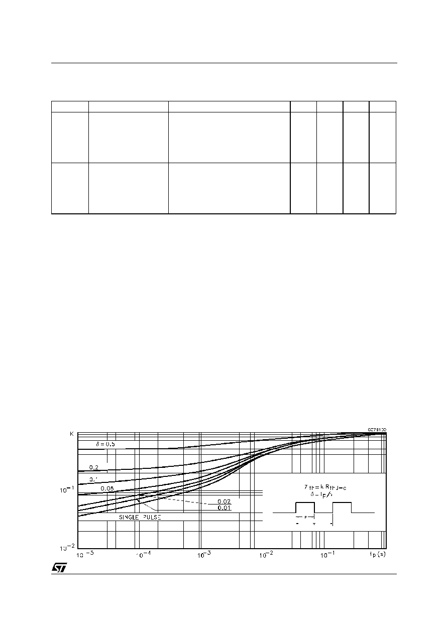
Thermal Impedance
STGP7NB60H
3/8
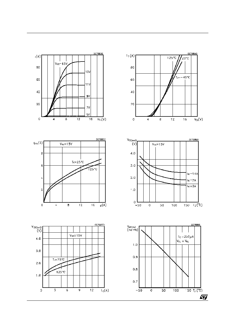
Output Characteristics
Transconductance
Collector-Emitter On Voltage vs Collector Current
Transfer Characteristics
Collector-Emitter On Voltage vs Temperature
Gate Threshold vs Temperature
STGP7NB60H
4/8
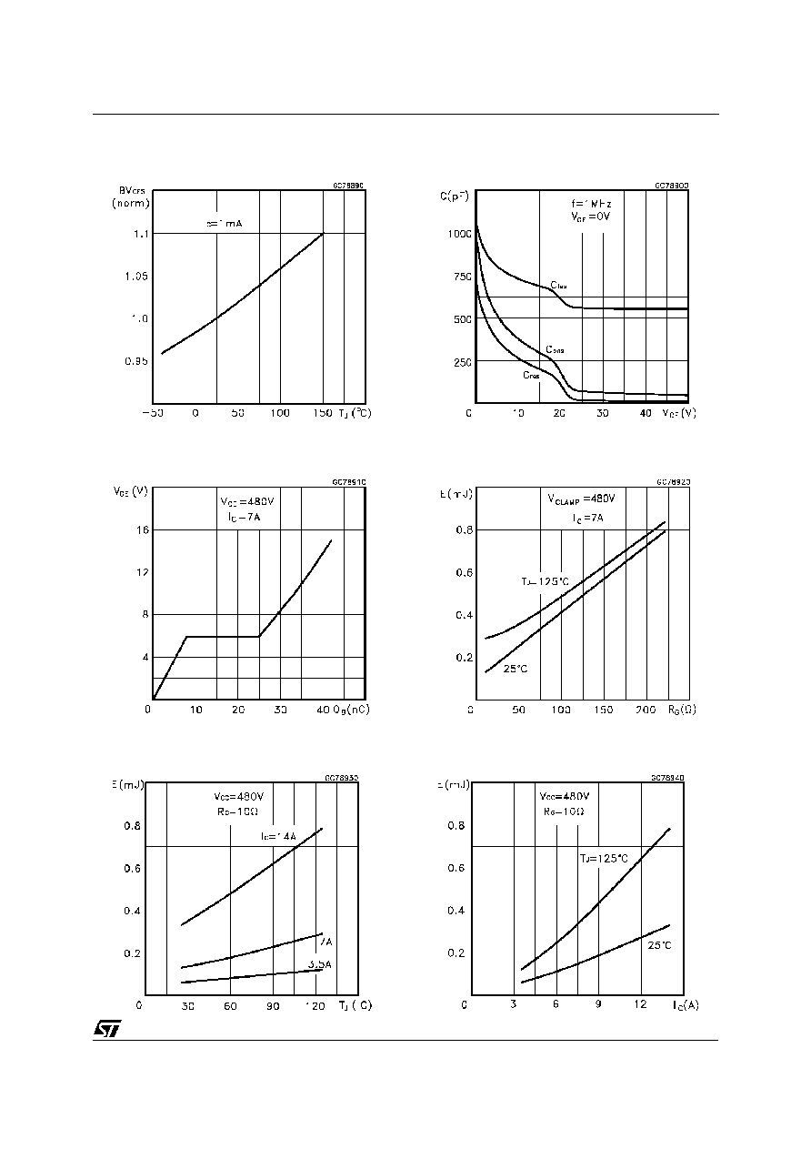
Normalized Breakdown Voltage vs Temperature
Gate Charge vs Gate-Emitter Voltage
Total Switching Losses vs Temperature
Capacitance Variations
Total Switching Losses vs Gate Resistance
Total Switching Losses vs Collector Current
STGP7NB60H
5/8
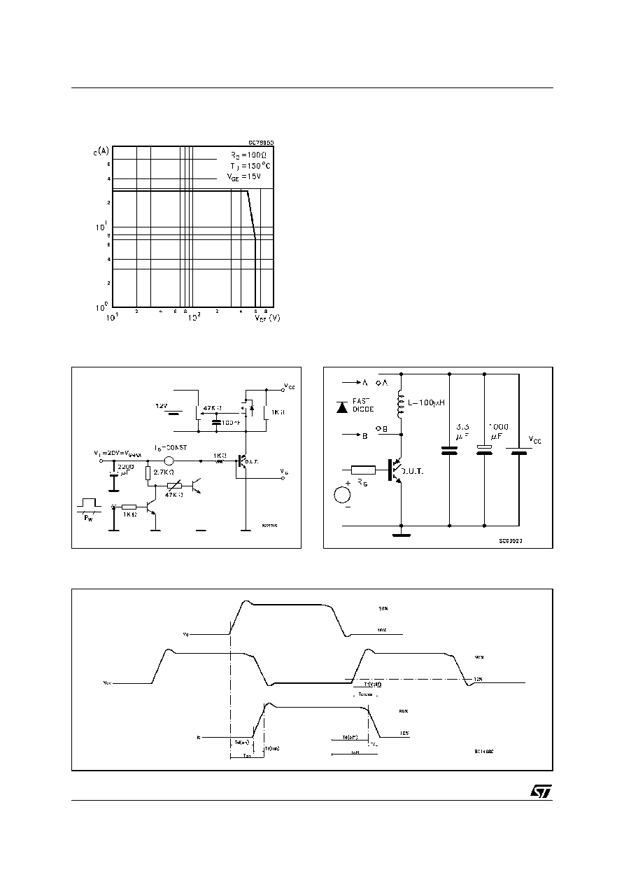
Switching Off Safe Operating Area
Fig. 1: Gate Charge test Circuit
Fig. 3: Switching Waveforms
Fig. 2: Test Circuit For Inductive Load Switching
STGP7NB60H
6/8
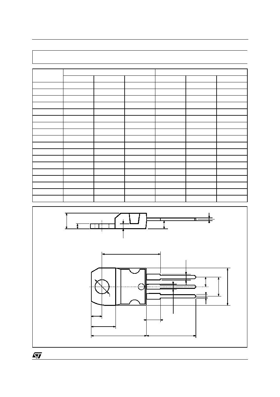
DIM.
mm
inch
MIN.
TYP.
MAX.
MIN.
TYP.
MAX.
A
4.40
4.60
0.173
0.181
C
1.23
1.32
0.048
0.051
D
2.40
2.72
0.094
0.107
D1
1.27
0.050
E
0.49
0.70
0.019
0.027
F
0.61
0.88
0.024
0.034
F1
1.14
1.70
0.044
0.067
F2
1.14
1.70
0.044
0.067
G
4.95
5.15
0.194
0.203
G1
2.4
2.7
0.094
0.106
H2
10.0
10.40
0.393
0.409
L2
16.4
0.645
L4
13.0
14.0
0.511
0.551
L5
2.65
2.95
0.104
0.116
L6
15.25
15.75
0.600
0.620
L7
6.2
6.6
0.244
0.260
L9
3.5
3.93
0.137
0.154
DIA.
3.75
3.85
0.147
0.151
L6
A
C
D
E
D1
F
G
L7
L2
Dia.
F1
L5
L4
H2
L9
F2
G1
TO-220 MECHANICAL DATA
P011C
STGP7NB60H
7/8

Information furnished is believ ed to be accurate and reliable. However, STMicroelectronics assumes no responsibil ity for the consequences
of use of such information nor for any infringement of patents or other rights of third parties which may result from its use. No license is
granted by implication or otherwise under any patent or patent rights of STMicroelectronics. Specific ation mentioned in this publication are
subjec t to change without notice. This publication supersedes and replaces all information previously supplied. STMicroelectronics products
are not authorized for use as critical components in life support devices or systems without express written approval of STMicroelectronics.
The ST logo is a trademark of STMicroelectronics
©
1999 STMicroelectronics ≠ Printed in Italy ≠ All Rights Reserved
STMicroelectronics GROUP OF COMPANIES
Australia - Brazil - China - Finland - France - Germany - Hong Kong - India - Italy - Japan - Malaysia - Malta - Morocco -
Singapore - Spain - Sweden - Switzerland - United Kingdom - U.S.A.
http://www.st.com
.
STGP7NB60H
8/8