1/11
July 2004
STGW20NC60VD
N-CHANNEL 30A - 600V
TO-247
Very Fast PowerMESHTM IGBT
Table 1: General Features
s
OFF LOSSES INCLUDE TAIL CURRENT
s
LOSSES INCLUDE DIODE RECOVERY
ENERGY
s
HIGH CURRENT CAPABILITY
s
HIGH FREQUENCY OPERATION UP TO 50
KHz
s
VERY SOFT ULTRA FAST RECOVERY
ANTIPARALLEL DIODE
s
LOWER C
RES
/C
IES
RATIO
s
NEW GENERATION PRODUCTS WITH
TIGHTER PARAMETER DISTRIBUTION
DESCRIPTION
Using the latest high voltage technology based on
a patented strip layout, STMicroelectronics has
designed an advanced family of IGBTs, the Pow-
erMESH
TM
IGBTs, with outstanding performances.
The suffix "V" identifies a family optimized for high
frequency applications.
APPLICATIONS
s
HIGH FREQUENCY INVERTERS
s
SMPS and PFC IN BOTH HARD SWITCH AND
RESONANT TOPOLOGIES
s
UPS
s
MOTOR DRIVERS
Table 2: Order Codes
Figure 1: Package
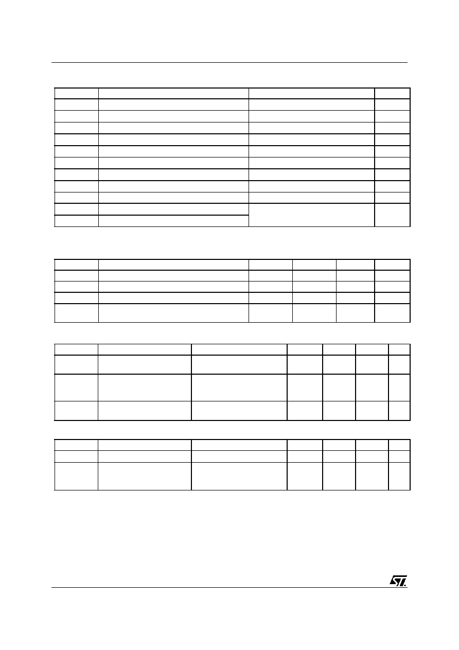
Figure 2: Internal Schematic Diagram
TYPE
V
CES
V
CE(sat)
(Max)
@25∞C
I
C
@100∞C
STGW20NC60VD
600 V
< 2.5 V
30 A
1
2
3
TO-247
Weight: 4.41gr ± 0.01
Max Clip Pressure: 150 N/mm
2
SALES TYPE
MARKING
PACKAGE
PACKAGING
STGW20NC60VD
GW20NC60VD
TO-247
TUBE
Rev. 4
STGW20NC60VD
2/11
Table 3: Absolute Maximum ratings
(1)Pulse width limited by max. junction temperature.
Table 4: Thermal Data
ELECTRICAL CHARACTERISTICS (T
CASE
=25∞C UNLESS OTHERWISE SPECIFIED)
Table 5: Off
Table 6: On
(#) Calculated according to the iterative formula:
Symbol
Parameter
Value
Symbol
V
CES
Collector-Emitter Voltage (V
GS
= 0)
600
V
V
ECR
Reverse Battery Protection
20
V
V
GE
Gate-Emitter Voltage
± 20
V
I
C
Collector Current (continuous) at 25∞C (#)
60
A
I
C
Collector Current (continuous) at 100∞C (#)
30
A
I
CM
(1)
Collector Current (pulsed)
100
A
I
f
Diode RMS Forward Current at T
C
= 25∞C
30
A
P
TOT
Total Dissipation at T
C
= 25∞C
200
W
Derating Factor
1.6
W/∞C
T
stg
Storage Temperature
≠ 55 to 150
∞C
T
j
Operating Junction Temperature
Min.
Typ.
Max.
Rthj-case
Thermal Resistance Junction-case (IGBT)
--
--
0.625
∞C/W
Rthj-case
Thermal Resistance Junction-case (Diode)
--
--
1.5
∞C/W
Rthj-amb
Thermal Resistance Junction-ambient
--
--
50
∞C/W
T
L
Maximum Lead Temperature for Soldering
Purpose (1.6 mm from case, for 10 sec.)
300
∞C
Symbol
Parameter
Test Conditions
Min.
Typ.
Max.
Unit
V
BR(CES)
Collectro-Emitter Breakdown
Voltage
I
C
= 1 mA, V
GE
= 0
600
V
I
CES
Collector-Emitter Leakage
Current (V
CE
= 0)
V
GE
= Max Rating
Tc=25∞C
Tc=125∞C
10
1
µA
mA
I
GES
Gate-Emitter Leakage
Current (V
CE
= 0)
V
GE
= ± 20 V , V
CE
= 0
± 100
nA
Symbol
Parameter
Test Conditions
Min.
Typ.
Max.
Unit
V
GE(th)
Gate Threshold Voltage
V
CE
= V
GE
, I
C
= 250 µA
3.75
5.75
V
V
CE(SAT)
Collector-Emitter Saturation
Voltage
V
GE
= 15 V, I
C
= 20A, Tj= 25∞C
V
GE
= 15 V, I
C
= 20A,
Tj= 125∞C
1.8
1.7
2.5
V
V
I
C
T
C
(
)
T
J MAX
T
C
≠
R
THJ
C
≠
V
CE SAT M AX
(
)
T
C
I
C
,
(
)
◊
--------------------------------------------------------------------------------------------------
=
3/11
STGW20NC60VD
ELECTRICAL CHARACTERISTICS (CONTINUED)
Table 7: Dynamic
Table 8: Switching On
2) Eon is the turn-on losses when a typical diode is used in the test circuit in figure 2. If the IGBT is offered in a package with a co-pack diode,
the co-pack diode is used as external diode. IGBTs & DIODE are at the same temperature (25∞C and 125∞C)
Table 9: Switching Off
(3)Turn-off losses include also the tail of the collector current.
Symbol
Parameter
Test Conditions
Min.
Typ.
Max.
Unit
g
fs
(1)
Forward Transconductance
V
CE
= 15 V
,
I
C
= 20 A
15
S
C
ies
C
oes
C
res
Input Capacitance
Output Capacitance
Reverse Transfer
Capacitance
V
CE
= 25V, f = 1 MHz, V
GE
= 0
2200
225
50
pF
pF
pF
Q
g
Q
ge
Q
gc
Total Gate Charge
Gate-Emitter Charge
Gate-Collector Charge
V
CE
= 390 V, I
C
= 20 A,
V
GE
= 15V,
(see Figure 21)
100
16
45
140
nC
nC
nC
I
CL
Turn-Off SOA Minimum
Current
V
clamp
= 480 V
,
Tj = 150∞C
R
G
= 10
,
V
GE
= 15V
100
A
Symbol
Parameter
Test Conditions
Min.
Typ.
Max.
Unit
t
d(on)
t
r
(di/dt)
on
Eon
(2)
Turn-on Delay Time
Current Rise Time
Turn-on Current Slope
Turn-on Switching Losses
V
CC
= 390 V, I
C
= 20 A
R
G
= 3.3
, V
GE
= 15V, Tj= 25∞C
(see Figure 19)
31
11
1600
220
300
ns
ns
A/µs
µJ
t
d(on)
t
r
(di/dt)
on
Eon
(2)
Turn-on Delay Time
Current Rise Time
Turn-on Current Slope
Turn-on Switching Losses
V
CC
= 390 V, I
C
= 20 A
R
G
= 3.3
, V
GE
= 15V, Tj=
125∞C
(see Figure 19)
31
11.5
1500
450
ns
ns
A/µs
µJ
Symbol
Parameter
Test Conditions
Min.
Typ.
Max.
Unit
t
r
(V
off
)
Off Voltage Rise Time
V
cc
= 390 V, I
C
= 20 A,
R
GE
= 3.3
, V
GE
= 15 V
T
J
= 25 ∞C
(see Figure 19)
28
ns
t
d
(
off
)
Turn-off Delay Time
100
ns
t
f
Current Fall Time
75
ns
E
off
(3)
Turn-off Switching Loss
330
450
µ
J
E
ts
Total Switching Loss
550
750
µ
J
t
r
(V
off
)
Off Voltage Rise Time
V
cc
= 390 V, I
C
= 20 A,
R
GE
= 3.3
, V
GE
= 15 V
Tj = 125 ∞C
(see Figure 19)
66
ns
t
d
(
off
)
Turn-off Delay Time
150
ns
t
f
Current Fall Time
130
ns
E
off
(3)
Turn-off Switching Loss
770
µ
J
E
ts
Total Switching Loss
1220
µ
J

STGW20NC60VD
4/11
Table 10: Collector-Emitter Diode
Symbol
Parameter
Test Conditions
Min.
Typ.
Max.
Unit
V
f
Forward On-Voltage
I
f
= 10 A
I
f
= 10 A, Tj = 125 ∞C
1.3
1
2.0
V
V
t
rr
t
a
Q
rr
I
rrm
S
Reverse Recovery Time
Reverse Recovery Charge
Reverse Recovery Current
Softness factor of the diode
I
f
= 20 A ,V
R
= 40 V,
Tj = 25∞C, di/dt = 100 A/
µ
s
(see Figure 22)
44
32
66
3
0.375
ns
ns
nC
A
t
rr
t
a
Q
rr
I
rrm
S
Reverse Recovery Time
Reverse Recovery Charge
Reverse Recovery Current
Softness factor of the diode
I
f
= 20 A ,V
R
= 40 V,
Tj =125∞C, di/dt = 100 A/
µ
s
(see Figure 22)
88
56
237
5.4
0.57
ns
ns
nC
A
5/11
STGW20NC60VD
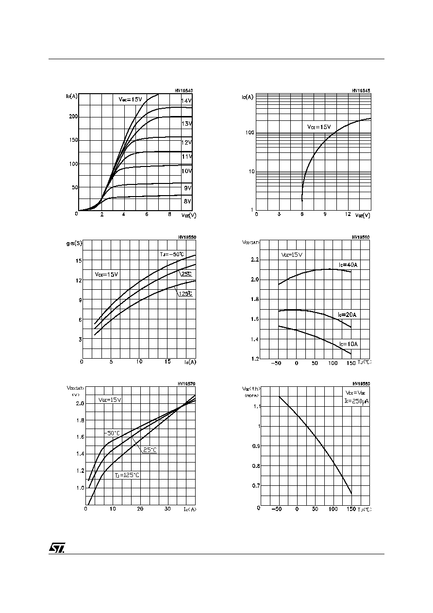
Figure 3: Output Characteristics
Figure 4: Transconductance
Figure 5: Collector-Emitter On Voltage vs Col-
lector Current
Figure 6: Transfer Characteristics
Figure 7: Collector-Emitter On Voltage vs Tem-
perature
Figure 8: Normalized Gate Threshold vs Tem-
perature