1/9
August 2003
STGW40NC60V
N-CHANNEL 50A - 600V
TO-247
Hyper Fast PowerMESHTM IGBT
s
HIGH INPUT IMPEDANCE
s
OFF LOSSES INCLUDE TAIL CURRENT
s
LOW GATE CHARGE
s
HIGH CURRENT CAPABILITY
s
VERY HIGH FREQUENCY OPERATION
s
CO-PACKAGED WITH TURBOSWITCH
ANTIPARALLEL DIODE
DESCRIPTION
Using the latest high voltage technology based on a
patented strip layout, STMicroelectronics has
designed an advanced family of IGBTs, the
PowerMESH
TM
IGBTs, with outstanding
performances. The suffix "V" identifies a family
optimized for high frequency welding and SMPS
applications.
APPLICATIONS
s
HIGH FREQUENCY INVERTERS
s
SMPS and PFC IN BOTH HARD SWITCH AND
RESONANT TOPOLOGIES
s
UPS
s
WELDING
ORDERING INFORMATION
TYPE
V
CES
V
CE(sat)
(Max)@25∞C
I
C
@100∞C
STGW40NC60V
600 V
< 2.5
V
50 A
SALES TYPE
MARKING
PACKAGE
PACKAGING
STGW40NC60V
GW40NC60V
TO-247
TUBE
TO-247
1
2
3
INTERNAL SCHEMATIC DIAGRAM
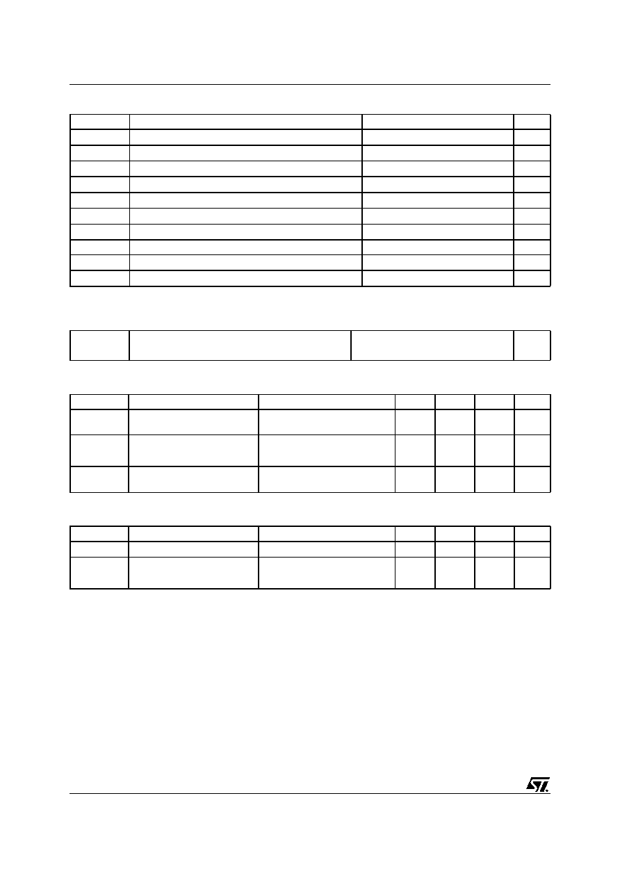
STGW40NC60V
2/9
ABSOLUTE MAXIMUM RATINGS
( )
Pulse width limited by safe operating area
THERMAL DATA
ELECTRICAL CHARACTERISTICS (T
CASE
= 25 ∞C UNLESS OTHERWISE SPECIFIED)
OFF
ON (1)
Symbol
Parameter
Value
Unit
V
CES
Collector-Emitter Voltage (V
GS
= 0)
600
V
V
ECR
Emitter-Collector Voltage
20
V
V
GE
Gate-Emitter Voltage
± 20
V
I
C
Collector Current (continuous) at T
C
= 25∞C
80
A
I
C
Collector Current (continuous) at T
C
= 100∞C
50
A
I
CM
( )
Collector Current (pulsed)
220
A
P
TOT
Total Dissipation at T
C
= 25∞C
260
W
Derating Factor
2.6
W/∞C
T
stg
Storage Temperature
≠ 55 to 125
∞C
T
j
Max. Operating Junction Temperature
125
∞C
Rthj-case
Thermal Resistance Junction-case Max
0.385
∞C/W
Rthj-amb
Thermal Resistance Junction-ambient Max
30
∞C/W
Symbol
Parameter
Test Conditions
Min.
Typ.
Max.
Unit
V
BR(CES)
Collector-Emitter Breakdown
Voltage
I
C
= 1 mA, V
GE
= 0
600
V
I
CES
Collector cut-off
(V
GE
= 0)
V
CE
= Max Rating, T
C
= 25 ∞C
250
µA
V
CE
= Max Rating, T
C
= 125 ∞C
1000
µA
I
GES
Gate-Emitter Leakage
Current (V
CE
= 0)
V
GE
= ±20 V , V
CE
= 0
±250
nA
Symbol
Parameter
Test Conditions
Min.
Typ.
Max.
Unit
V
GE(th)
Gate Threshold Voltage
V
CE
= V
GE
, I
C
= 250 µA
3
4
5
V
V
CE(sat)
Collector-Emitter Saturation
Voltage
V
GE
= 15 V, I
C
= 40 A, Tj =25∞C
1.92
2.5
V
V
GE
=15 V, I
C
= 40 A, Tj =125∞C
1.7
V
3/9
STGW40NC60V
ELECTRICAL CHARACTERISTICS (CONTINUED)
DYNAMIC
SWITCHING ON
SWITCHING OFF
Note: 1. Pulsed: Pulse duration = 300 µs, duty cycle 1.5 %.
2. Pulse width limited by max. junction temperature.
(**)Losses include Also the Tail (Jedec Standardization)
Symbol
Parameter
Test Conditions
Min.
Typ.
Max.
Unit
g
fs
Forward Transconductance
V
CE
= 25 V
,
I
C
= 20 A
20
S
C
ies
Input Capacitance
V
CE
= 25 V, f= 1 MHz, V
GE
= 0
4550
pF
C
oes
Output Capacitance
350
pF
C
res
Reverse Transfer
Capacitance
105
pF
Q
g
Q
ge
Q
gc
Total Gate Charge
Gate-Emitter Charge
Gate-Collector Charge
V
CE
= 480 V, I
C
= 40 A,
V
GE
= 15 V
220
30
105
nC
nC
nC
I
CL
Latching Current
V
clamp
= 480 V
,
Tj = 125∞C
R
G
= 10
220
A
Symbol
Parameter
Test Conditions
Min.
Typ.
Max.
Unit
t
d(on)
t
r
Turn-on Delay Time
Rise Time
V
CC
= 480 V, I
C
= 40 A
R
G
= 10
, V
GE
= 15 V
45
27
ns
ns
(di/dt)
on
Eon
Turn-on Current Slope
Turn-on Switching Losses
V
CC
= 480 V, I
C
= 40 A
R
G
= 10
,
V
GE
= 15 V,
Tj =125∞C
1150
800
A/µs
µJ
Symbol
Parameter
Test Conditions
Min.
Typ.
Max.
Unit
t
r
(V
off
)
Off Voltage Rise Time
V
cc
= 480 V, I
C
= 40 A,
R
GE
= 10
, V
GE
= 15 V
T
J
= 25 ∞C
37
ns
t
d
(
off
)
Delay Time
270
ns
t
f
Fall Time
70
ns
E
off
(**)
Turn-off Switching Loss
1120
µ
J
E
ts
Total Switching Loss
1880
µ
J
t
r
(V
off
)
Off Voltage Rise Time
V
cc
= 480 V, I
C
= 40 A,
R
GE
= 10
, V
GE
= 15 V
Tj = 125 ∞C
67
ns
t
d
(
off
)
Delay Time
325
ns
t
f
Fall Time
120
ns
E
off
(**)
Turn-off Switching Loss
1600
µ
J
E
ts
Total Switching Loss
2400
µ
J
STGW40NC60V
4/9
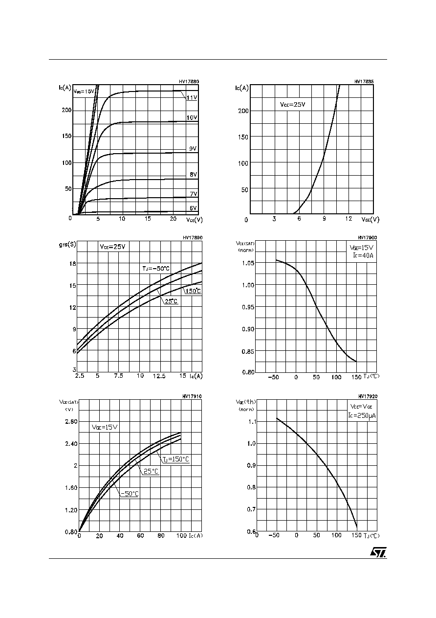
Gate Threshold vs Temperature
Collector-Emitter On Voltage vs Collector Current
Normalized Collector-Emitter On Voltage vs Temp.
Transconductance
Transfer Characteristics
Output Characteristics
5/9
STGW40NC60V
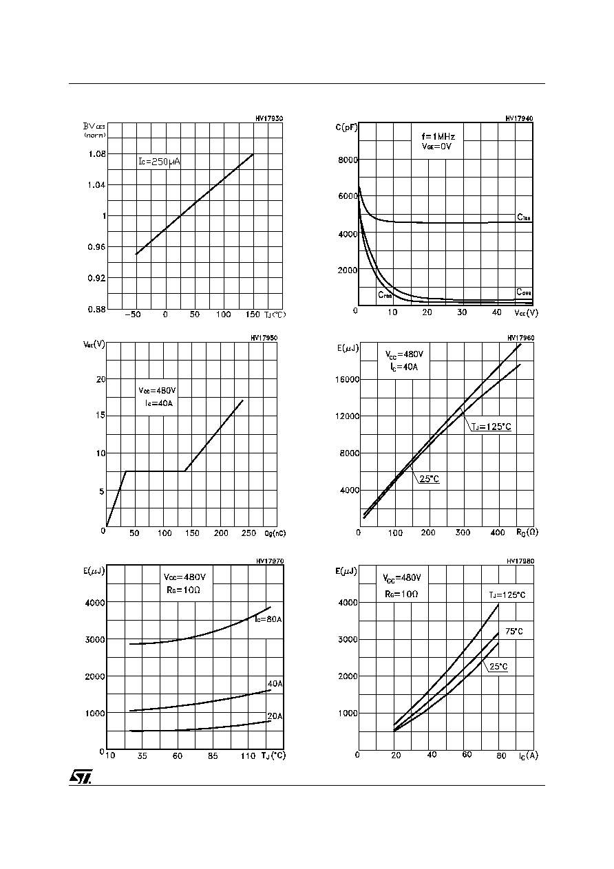
Total Switching Losses vs Collector Current
Total Switching Losses vs Temperature
Total Switching Losses vs Gate Resistance
Gate Charge vs Gate-Emitter Voltage
Capacitance Variations
Normalized Breakdown Voltage vs Temperature