 | –≠–ª–µ–∫—Ç—Ä–æ–Ω–Ω—ã–π –∫–æ–º–ø–æ–Ω–µ–Ω—Ç: STI5500 | –°–∫–∞—á–∞—Ç—å:  PDF PDF  ZIP ZIP |
October 1997
SUMMARY
This is advance information on a new product now in development or undergoing evaluation. Details are subject to change without notice.
CO
NFI
DE
NTI
AL
STi5500
SET TOP BOX / DVD BACKEND DECODER
WITH INTEGRATED HOST PROCESSOR
.
ENHANCED 32-BIT VL-RISC CPU
- FAST INTEGER/BIT OPERATION AND
VERY HIGH CODE DENSITY
.
HIGH PERFORMANCE MEMORY/CACHE
SUBSYSTEM
- 2KBYTES INSTRUCTION CACHE, 2KBYTES
SRAM, 2KBYTES DATA CACHE/SRAM
- 160MBYTES/S BANDWIDTH
.
COMBINED VIDEO AND AUDIO DECODER CORE
- VIDEO DECODER FULLY SUPPORTS
MPEG-2 MP@ML
- MEMORY REDUCTION - PAL MP@ML IN
12MBITS
- 2 TO 8 BIT PER PIXEL OSD OPTIONS
- LETTERBOX (16:9) DISPLAY FORMAT
- HORIZONTAL AND VERTICAL RESIZING
FUNCTIONS
- AUDIO DECODER SUPPORTS LAYERS
1 AND 2 OF MPEG, INTERFACE TO
EXTERNAL DOLBY AC-3
TM
DECODER
.
PAL/NTSC ENCODER
- MACROVISION
TM
VERSION 7.01/6.1
COMPATIBLE
- TELETEXT, AND CLOSED CAPTION
- SIMULTANEOUS OUTPUT OF RGB, CVBS
AND COMPONENT VIDEO
.
HIGH PERFORMANCE SDRAM MEMORY
INTERFACE
- SUPPORTS 1 OR 2 16MBIT 100MHz SDRAMS
- ACCESSIBLE BY MPEG DECODER, CPU
AND DMAS
- HIGH BANDWIDTH ACCESS FROM CPU
ALLOWS HIGH PERFORMANCE OSD
OPERATIONS
.
PROGRAMMABLE MEMORY INTERFACE
- 4 BANKS EACH 8/16 BITS WIDE
- S U P P O R T F O R M I X E D M E M O R Y ,
P E R I P H ERALS, DRAM AND POWER PC
.
LINK INTERFACE
- SERIAL INPUT
- SUPPORTS DSS, DVB, AND DVD
BITSTREAMS
- 32 PIDS SUPPORTED
- DES AND DVB DESCRAMBLERS
- 32 SI/PSI FILTERS OF 16 BYTES
.
VECTORED INTERRUPTS - 8 PRIORITIZED
LEVELS
.
DMA ENGINES/INTERFACES
- 2 UARTS, 1 I
2
C CONTROLLER, 3 PWM
OUTPUTS, 3 TIMERS, 3 CAPTURE TIMERS
- 24 BITS OF PIO SHARED WITH SERIAL
INTERFACES
- OS LINK INTERFACE
- BLOCK MOVE DMA, 2 MPEG DMAS
- TELETEXT INTERFACE
.
PROFESSIONAL TOOLSET SUPPORT
- ANSI C COMPILER AND LIBRARIES
- INQUEST ADVANCED DEBUGGING TOOLS
.
NON-INTRUSIVE DEBUG CONTROLLER
- HARDWARE BREAKPOINTS
- REAL TIME TRACE
.
208 PIN PQFP PACKAGE
DESCRIPTION
The STi5500 is the first of a new generation of
integrated multimedia decoder engines for set top
box and DVD applications. It offers a high level of
integration by reducing the complete set top box
decoding chain from Transport Demux to
PAL/NTSC Encoder onto one chip. At the same time
it dramatically enhances CPU and Graphics per-
formance, and cuts down total system memory cost.
PQFP208
(Plastic Quad Flat Pack)
ORDER CODE : STi5500
1/11

CO
NFI
DE
NTI
AL
I - PIN DESCRIPTION
I.1 - Pin Connections
120
119
118
117
116
115
114
113
112
111
110
109
108
107
106
105
2
0
8
2
0
6
2
0
5
2
0
4
136
135
134
133
132
131
130
129
128
127
126
125
124
123
122
121
140
139
138
137
143
142
141
147
146
145
144
149
148
153
152
151
150
156
155
154
2
0
3
2
0
2
2
0
1
2
0
0
1
9
9
1
9
8
1
9
7
1
9
6
1
9
5
1
9
4
1
9
3
1
9
2
1
9
1
1
9
0
1
8
9
1
8
8
1
8
7
1
8
6
1
8
5
1
8
4
1
8
3
1
8
2
1
8
1
1
8
0
1
7
9
1
7
8
1
7
7
1
7
6
1
7
5
1
7
4
1
7
3
1
7
2
1
7
1
1
7
0
1
6
9
1
6
8
1
6
7
1
6
6
1
6
5
1
6
4
1
6
3
1
6
0
1
5
9
1
5
8
1
5
7
1
6
2
1
6
1
2
0
7
1
2
3
4
5
6
7
8
9
10
11
12
13
14
15
16
17
18
19
20
21
22
23
24
25
26
27
28
29
30
31
32
33
34
35
36
37
38
39
40
41
42
43
44
45
46
47
48
49
50
51
52
5
3
5
4
5
5
5
6
5
7
5
8
5
9
6
0
6
1
6
2
6
3
6
4
6
5
6
6
6
7
6
8
6
9
7
0
7
1
7
2
7
3
7
4
7
5
7
6
7
7
7
8
7
9
8
0
8
1
8
2
8
3
8
4
8
5
8
6
8
8
8
9
9
0
9
1
9
2
8
7
9
3
9
4
9
5
9
6
9
7
9
8
1
0
0
1
0
1
1
0
2
1
0
3
1
0
4
9
9
V
DD
PIO3[7]
PIO2[0]
GND
PIO2[3]
PIO2[4]
PIO2[5]
PIO2[7]
PIO1[0]
PIO1[2]
PIO1[5]
PIO1[6]
PIO1[7]
PIO4[7]
PIO0[0]
PIO0[3]
PIO0[4]
V
DD
GND
PIO0[5]
PIO0[6]
PIO0[7]
IRQ[0]
IRQ[1]
IRQ[2]
BRM0
BRM1
BRM2
NOT_RST
SDAV_CLK (PI394_CLK)
SDAV_CLK (PI394_DATA)
SDAV_DIR (PI394_CLK)
OSC_IN
V
DD
GND
F_DATA
F_B_BCLK
F_P_CLK
F_ERR
NRSS_CLK
NRSS_OUT
NRSS_IN
PCM_CLKOUT (A_C_STB)
PCM_DATA (A_C_DATA)
PCM_CLKIN
A_C_REQ
A_PTS_STB
V
DD
GND
NOTHSYNC
ODD_OR_EVEN
V
D
D
A
_
0
V
S
S
A
_
0
B
_
O
U
T
G
_
O
U
T
R
_
O
U
T
I
_
R
E
F
_
D
A
C
_
R
G
V
_
R
E
F
_
D
A
C
_
R
G
V
D
D
A
_
1
V
S
S
A
_
1
Y
_
O
U
T
C
_
O
U
T
C
V
_
O
U
T
V
_
R
E
F
_
D
A
C
_
Y
C
I
_
R
E
F
_
D
A
C
_
Y
C
V
D
D
G
N
D
A
D
[
4
]
A
D
[
5
]
A
D
[
6
]
A
D
[
7
]
A
D
[
8
]
A
D
[
9
]
V
D
D
M
E
M
C
L
K
O
U
T
G
N
D
A
D
[
0
]
A
D
[
1
]
A
D
[
2
]
A
D
[
3
]
A
D
[
1
1
]
A
D
[
1
0
]
N
O
T
_
S
D
C
S
[
0
]
N
O
T
_
S
D
C
S
[
1
]
V
D
D
G
N
D
N
O
T
_
S
D
R
A
S
N
O
T
_
S
D
C
A
S
N
O
T
_
S
D
W
E
D
Q
M
L
D
Q
[
0
]
D
Q
[
1
]
D
Q
[
2
]
V
D
D
G
N
D
D
Q
[
3
]
D
Q
[
4
]
D
Q
[
5
]
D
Q
[
6
]
D
Q
[
7
]
V
D
D
G
N
D
M
E
M
C
L
K
I
N
DQMU
DQ[8]
DQ[9]
DQ[10]
DQ[11]
V
DD
GND
DQ[12]
DQ[13]
DQ[14]
DQ[15]
AUXCLK
OSD_ACTIVE
PIXCLK_27MHz
V
DD
GND
NOT_WE0
NOT_WE1
NOT_OE
NOT_CE1
NOT_CE2
NOT_CE3
NOT_RAS0
NOT_RAS1
NOT_CAS0
V
DD
GND
NOT_CAS1
READnotWRITE
DMAXFER
NOT_CSDXX
READY
CPU_CLK (PPC_CLK)
N_PPC_MOD
V
DD
GND
DATA[0]
DATA[1]
DATA[2]
DATA[3]
DATA[4]
DATA[5]
DATA[6]
DATA[7]
V
DD
GND
DATA[8]
DATA[9]
DATA[10]
DATA[11]
DATA[12]
DATA[13]
V
D
D
P
I
O
3
[
6
]
P
I
O
3
[
5
]
P
I
O
3
[
4
]
P
I
O
3
[
3
]
P
I
O
3
[
2
]
P
I
O
3
[
1
]
P
I
O
3
[
0
]
G
N
D
P
I
O
1
[
4
]
P
I
O
1
[
3
]
P
I
O
4
[
6
]
P
I
O
4
[
5
]
P
I
O
4
[
4
]
P
I
O
4
[
3
]
P
I
O
4
[
2
]
P
I
O
4
[
1
]
P
I
O
4
[
0
]
N
O
T
_
T
R
S
T
T
D
O
T
C
K
T
M
S
T
D
I
G
N
D
V
D
D
A
D
R
[
2
1
]
A
D
R
[
2
0
]
A
D
R
[
1
9
]
A
D
R
[
1
8
]
A
D
R
[
1
7
]
A
D
R
[
1
6
]
A
D
R
[
1
5
]
A
D
R
[
1
4
]
A
D
R
[
1
3
]
A
D
R
[
1
2
]
A
D
R
[
1
1
]
G
N
D
V
D
D
A
D
R
[
1
0
]
A
D
R
[
9
]
A
D
R
[
8
]
A
D
R
[
7
]
A
D
R
[
6
]
A
D
R
[
5
]
A
D
R
[
4
]
A
D
R
[
3
]
A
D
R
[
2
]
A
D
R
[
1
]
G
N
D
V
D
D
D
A
T
A
[
1
5
]
D
A
T
A
[
1
4
]
STi5500
PQFP208
(Top View)
LRCLK (A_WORD_CLK)
5
5
0
0
-
0
1
.
E
P
S
STi5500
2/11
CO
NFI
DE
NTI
AL
II - PIN DESCRIPTION (continued)
I.2 - Pin List
Pin
Name
Type
Function
SUPPLIES
1, 18, 34, 49, 67, 75, 86, 95,
102, 110, 119, 130, 139,
149, 159, 171, 184, 208
V
DD
Power Supply
4, 19, 35, 50, 68, 77, 87, 96,
103, 111, 120, 131, 140,
150, 160, 172, 185, 200
GND
Ground
53, 60
VDDA
Analog Power Supply for DENC
54, 61
VSSA
Analog Ground for DENC
VIDEO OUTPUT INTERFACE
57
R_OUT
O
Red Output
56
G_OUT
O
Green Output
55
B_OUT
O
Blue Output
63
C_OUT
O
Chroma Output
64
CV_OUT
O
Composite Video Output
62
Y_OUT
O
Luma Output
59
I_REF_DAC_RGB
I
DAC Current Reference
66
I_REF_DAC_YCC
I
DAC Current Reference
58
V_REF_DAC_RGB
I
DAC Voltage Reference
65
V_REF_DAC_YCC
I
DAC Voltage Reference
117
OSD_ACTIVE
I/O
OSD Active
118
PIXCLK_27MHz
I
System Clock Input
51
NOTHSYNC
I/O
Horizontal Sync
52
ODD_OR_EVEN
I/O
Vertical Sync
AC-3/MPEG1-2 AUDIO OUTPUT INTERFACE
43
PCM_CLKOUT / A_C_STB
O
(PCM Clock Out) or AC3 Data Strobe Data Out
44
PCM_DATA / A_C_DATA
O
PCM Data Out or AC3
45
PCM_CLKIN
I/O
PCM CLock In From VCXO
46
LRCLK / A-WORD_CLK
O
Left/Right Clock or AC3 Word Clock
47
A_C_REQ
I
AC3 Data Request
48
A_PTS_STB
I
AC3 Audio PTS Strobe
EXTERNAL INTERRUPTS
23, 25, 24
IRQ0-2
I
External Interrupts
PROGRAMMABLE I/O
15, 16, 17, 20, 21, 22
PIO-0 [0, 3-7]
I/O
General Purpose IO
9, 10, 198, 199, 11, 12, 13
PIO-1 [0, 2-7]
I/O
General Purpose IO
3, 5, 6, 7, 8
PIO-2 [0, 3-5,7]
I/O
General Purpose IO
201-207, 2
PIO-3 [0-7]
I/O
General Purpose IO
191-197, 14
PIO-4 [0-7]
I/O
General Purpose IO
JTAG INTERFACE
188
TCK
I
Test Clock
186
TDI
I
Test Data Input
189
TDO
O
Test Data Input
187
TMS
I
Test Mode Select
190
NOT_TRST
I
Test Reset
SYSTEM USE
28
BRM2
O
Modem Voltage Control
27
BRM1_OR_BOOTFROMROM
O/I
VCXO Control Audio BRM or Bootfromrom
During Reset
26
BRM0_OR_OSLINK_SEL
O/I
VCXO Control Video BRM or Configure Oslink
Pins
29
NOT_RST
I
Reset
116
AUXCLK
O
Auxilary Clock for Any Purpose
STi5500
3/11
CO
NFI
DE
NTI
AL
II - PIN DESCRIPTION (continued)
II.2 - Pin List (continued)
Pin
Name
Type
Function
SDRAM INTERFACE
78-81, 69, 70, 71, 72, 73,
74, 82, 83
AD[0:11]
O
SDRAM Address Bus
92, 93, 94, 97, 98, 99, 100,
101, 106, 107, 108, 109,
112-115
DQ[0:15]
I/O
SDRAM Data (Lower Byte)
84, 85
NOT_SDCS0-1
O
SDRAM Chip Selects
89
NOT_SDCAS
O
SDRAM CAS
88
NOT_SDRAS
O
SDRAM RAS
90
NOT_SDWE
O
SDRAM Write Enable
104
MEMCLKIN
I
SDRAM Memory Clock Input
76
MEMCLKOUT
O
SDRAM Memory Clock Output
91
DQML
O
DQ Mask Enable (Lower)
105
DQMU
O
DQ Mask Enable (Upper)
ROM AND EXTERNAL MICROPROCESSOR
161-170, 173-183
ADR[1:21]
I/O
External Memory Address Bus
141-148, 151-158
DATA[0:15]
I/O
External Memory Data Bus
128
NOT_RAS1_OR_HOLDREQ
O
DRAM RAS or Bus Request to External Micro
136
READY
O
Hold off External Micro
133
READNOTWRITE_OR_DMAACK
I/O
DRAM R/W Strobe or DMA Acknowledge from
External Micro
121, 122
NOT_WE[0:1]
I/O
Write Enable of SRAM
129
NOT_CAS0_OR_HOLDACK
O/I
DRAM CAS or Bus Grant from External Micro
132
NOT_CAS1_OR_NOT_DMAREQ
O
DRAM CAS or DMA Request (Ready) to
External Micro
124-126
NOT_CE[1:3]
O
Chip Select for Banks 1 - 3
135
NOT_CS
I
Chip Select to Access SDRAM
137
PPC_CLK
I
Power PC System Clock
127
NOT_RAS0_OR_NOT_CE4
O
DRAM RAS or Chip Select for Bank 0
134
DMAXFER
I
DMA Transfer Control from External Micro
138
NOT_PPC_MODE
I
Presence of Power PC
123
NOT_OE
I/O
Output Enable of RAM / ROM
SDAV INERFACE
30
SDAV_CLK
I/O
Data Strobe / CLK
31
SDAV_DATA
I/O
Data Line
32
SDAV_DIR
O
Direction for Transmit Truefer Transmit, Pulse
for Receive
33
OSC_IN
I/O
49.152MHz Crystal Input
NRSS INTERFACE
40
NRSS_CLK
O
NRSS Serial Clock
42
NRSS_IN
I
NRSS Serial Data Input
41
NRSS_OUT
O
NRSS Serial Data Output
P1394 INTERFACE
30
P1394_CLK
I/O
Data Strobe / CLK
31
P1394_DATA
I/O
Data Line
32
P1394_P_CLK
I/O
Packet Clock
STi5500
4/11
CO
NFI
DE
NTI
AL
II - BLOCK DIAGRAM
ST20 CPU
INTERRUPT
CONTROLLER
EMI
MPEG AUDIO
DECODER
AC-3 I/F
PAL/NTSC
ENCODER
TELETEXT
INTERFACE
MPEG VIDEO
DECODER
BLOCK MOVE
DMA
2 MPEG
DMAs
LINK
INTERFACE
2K
INSTRUCTION
CACHE
2K DATA
CACHE AND
2K SRAM
OS LINK
2 UART
1 I
2
C
PIO
3 PWM
DIAGNOSTICS
CONTROLLER
AND SYSTEM
SERVICES
2
SMARTCARD
INTERFACES
(ASC)
5
5
0
0
-
0
2
.
E
P
S
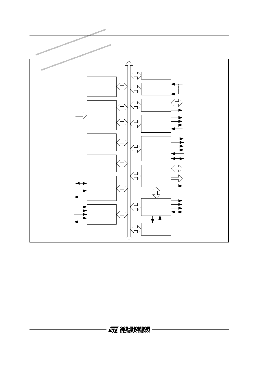
Figure 1 : General Block Diagram
STi5500
5/11

CO
NFI
DE
NTI
AL
III - INTERNAL CIRCUIT DESCRIPTION
A general block diagram for the STi5500 is shown
is Figure 1.
The performance offered by the ST20 32-bit micro-
core allows the following operations to be per-
formed in software :
1 Device drivers for Video, Audio and Sub-picture
Decoders
2 Audio/Video/Subpicture synchronisation
3 System management functions
4 Electronic program guide
5 Conditional access module
The use of a 32-bit CPU enables advanced graph-
ics routines to be employed for on-screen display
functions, allowing fast turnaround system up-
grades.
III.1 - The ST20 32-bit CPU
The ST20 micro-core family has been developed by
SGS-THOMSON Microelectronics to provide the
tools and building blocks to enable the development
of highly integrated application-specific 32-bit de-
vices at the lowest cost and fastest time to market.
The ST20 macrocell library includes the ST20Cx
family of 32-bit VL-RISC (variable length reduced
instruction set computer) micro-cores, embedded
memories, standard peripherals, I/O, controllers
and ASICs.
The STi5500 uses the ST20 macrocell library to
provide all of the dedicated hardware modules
required in a set top box or DVD system.
These include :
- High performance internal SRAM and cache sub-
system,
- I
2
C interfaces to other devices in the set top box,
- UART serial I/O interface to modem and auxiliary
ports,
- Interrupt controller for internal and external interrupts,
- DMA to MPEG audio and video device(s),
- External memory interface supporting DRAM,
EPROM and peripherals,
- PWM/timer module for control of system clock VCXOs,
- Programmable I/O pins,
- Smart card interfaces.
III.2 - MPEG-2 Video/Audio Decoder
The video decoder implemented in the STi5500
uses a patented memory reduction/bandwidth re-
duction scheme to offer the user the best band-
width/memory size compromise.
The algorithm is lossless and uses "on-the-fly"
decoding to reduce the memory requirements to
2 frame buffers in memory size reduction mode.
When used in bandwidth reduction mode the mem-
ory usage is the normal three buffers but the band-
width required by the decoder is significantly re-
duced over a classical implementation.
In summary the features of this decoder core are :
- Video decoder fully supports MPEG-2 Main Pro-
file/Main Level (MP@ML),
- Memory reduction architecture allows sharing of
single 16MBit SDRAM between MPEG decoding,
micro and transport functions - memory expand-
able to 32Mbits of SDRAM,
- Letterbox filter,
- Horizontal and vertical image re-sizing,
- 2 to 8 bit OSD (6-bit luma resolution, 4-bit chroma
resolution),
- Accepts MPEG-2 Program Streams, PES and
MPEG-1 system streams,
- Automatic error concealment.
The output from the video decoder is fed directly to
a PAL/NTSC encoder unit generating simultane-
ously a composite video signal, component Y/C
and RGB for each of the two standards.
The signals can be optionally encoded following
the Macrovision
TM
7.01/6.1 specification if the user
has a licence to use the technology. The digital
encoder cell is also capable of encoding into the
composite signal teletext and closed caption infor-
mation.
The audio decoder performs MPEG levels 1 and
II decoding and is functionally equivalent to the
STi3520A audio decoder. The STi5500 has a dedi-
cated interface to an external Dolby AC3 decoder
whilst allowing audio buffering to be performed in
the 16 Mbit SDRAM.
III.3 - High Quality Graphics
The graphics performance of the STi5500 supports
the new requirements for intelligent program
guides and interactive applications.
The display interface supports up to 256 colours for
each OSD region and a transparency feature al-
lows mixing of video with the OSD. Fast access
graphics and many other additional features are
available and are supported by a graphics library.
Excellent system performance is obtained by
closely coupling the high performance RISC proc-
essor and cache with the MPEG audio/video core
and display memory.
Low latency RISC access and DMA engines allow
rapid construction of bit maps. DVD graphics are
also supported by an integrated sub picture de-
coder. Pan and scan and letterbox output are pro-
vided for 16:9 applications.
STi5500
6/11

CO
NFI
DE
NTI
AL
III.4 - External Memory
III - INTERNAL CIRCUIT DESCRIPTION (continued)
The STi5500 has been designed to minimize sys-
tem costs. The external memory interface contains
a zero glue logic DRAM controller and a low-cost
16-bit EPROM interface.
The STi5500 applies a unique memory architecture
which consolidates the system, on-screen display,
audio and video memory into a single memory chip.
Moreover, a patented memory management algo-
rithm allows the STi5500 to decode an MPEG2 MP
@ ML bitstream with CCIR601 NTSC pictures in
only 10.5 Mbits and with CCIR601 PAL pictures in
only 12MBits, with absolutely no impact on the
picture quality.
If 16MBits SDRAM is attached to the STi5500, then
4 Mbits or more are free for other purposes such
as full screen high resolution graphics and proces-
sor use. A second optional 16Mbit SDRAM can also
be added for applications which require more
graphics features such as full screen still image
display or processor memory.
The STi5500 also has a generic processor inter-
face allowing DMA access to the SDRAM memory
by an external processor.
The SDRAM memory interface directly supports
100MHz SDRAMs providing the very high band-
widths to support MPEG decoding and display,
OSD drawing and display, and general system use.
Furthermore, the ST20 VL-RISC micro-core has
the highest code density of any 32-bit CPU, leading
to the lowest cost program ROM.
III.5 - STi5500 Functional Description
III.5.1 - STi5500 Functional Modules
Figure 1 shows the subsystem modules that com-
prise the STi5500. These modules are outlined
below and more detailed information is given in the
following chapters of this datasheet.
III.5.2 - CPU
The Central Processing Unit (CPU) on the STi5500
is the ST20-C2 32-bit processor core. It contains
instruction processing logic, instruction and data
pointers and an operand register. It directly ac-
cesses the high speed on-chip SRAM memory,
which can store data or programs, and uses the
Caches to reduce access time to off chip program
and data memory. The processor can access mem-
ory via the general purpose External Memory Inter-
face (EMI) or via the SDRAM EMI which is shared
with the MPEG decoder.
III.5.3 - Memory Subsystem
The STi5500 on-chip SRAM memory system pro-
vides 160Mbytes/s internal data bandwidth, sup-
porting pipelined 2-cycle internal memory access
at 25 ns cycle times. The STi5500 memory system
consists of 2 Kbytes of SRAM, 2Kbytes of instruc-
tion cache, a 2Kbyte data cache that can be pro-
grammed to be SRAM, and an external memory
interface (EMI).
The STi5500 product has 2 Kbytes of on-chip
SRAM. The advantage of this is the ability to store
time critical code on chip, for instance interrupt
routines, software kernels or device drivers, and
even frequently used data without these being
flushed from the caches.
The instruction and data caches are direct mapped
with a write-back system for the data cache and
support burst accesses to the external memories
for refill and write-back which are effective for in-
creasing performance with page-mode and
SDRAM memories.
The STi5500 EMI controls access to the external
memory and peripherals while the SDRAM EMI
provides access to the SDRAM buffer for the
MPEG decoders, ST20 and DMA peripherals.
The STi5500 EMI can access a 16 Mbyte (or
greater if DRAM is used) physical address space
in each of the four general purpose memory banks,
and provides sustained transfer rates of up to
80Mbytes/s.
Peripherals that support an asynchronous data
acknowledge are supported as is an external
PowerPC which can share the bus with the
STi5500 and access the SDRAM buffer through
the device.
High memory bandwidths up to 200Mbytes/s can
be supported by the SDRAM EMI (see Figure 2).
The STi5500 internal memory interconnect provides
buffering and arbitration of memory access requests to
sustain very high throughput of memory accesses.
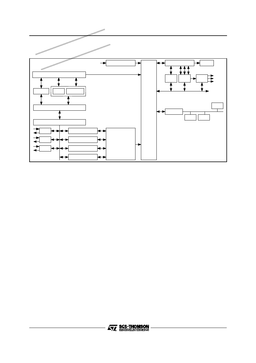
Figure 1 STi5500 architectural block diagram.
STi5500
7/11
CO
NFI
DE
NTI
AL
III.5.4 - System services module
The STi5500 system services module includes :
- phase locked loop (PLL) - accepts 27MHz input
and generates all the internal high frequency
clocks needed for the CPU and the OS-Link.
- Test access port - JTAG compatible,
- Diagnostics controller accessed via the JTAG
port providing :
- Bootstrapping during development,
- Hardware breakpoint and watchpoint,
- Real time trace,
- External LSA triggering support.
III.5.5 - Serial Communications
To facilitate the connection of this system the front
end device and other peripherals, two UARTs
(ASCs) are included in the device. The UARTs
provide an asynchronous serial interface. The
UART can be programmed to support a range of
baud rates and data formats, for example, data
size, stop bits and parity. Two synchronous serial
communications (SSC) interfaces are provided on
the device. These can be used for a remote control
device for example via an I2C or SPI bus.
III.5.6 - Interrupt Subsystem
The STi5500 interrupt subsystem supports eight
prioritized interrupt levels. Four external interrupt
pins are provided. Level assignment logic allows
any of the internal or external interrupts to be as-
signed and, if necessary, share any interrupt level.
III.5.7 - Link Interface
The link interface is an integrated transport stream
processor which accepts either DSS or DVB
streams on a serial interface with a front-end de-
vice. The interface performs the demultiplexing
operations with no interaction from the ST20. In
summary the features of the interface are :
- Framing of transport packets (SYNC byte detection),
- PID filtering of up to 32 PIDs,
- Descrambling to DVB/DES standard - transport
or PES level (DVB),
- Adaptation field parsing - detection and time
stamping. System time clock adjustment handled
by software.
- Section filtering - 32 filters,
- Demultiplexing of transport stream by PID,
- DMA and buffering of streams in memory with
communication to CPU of buffer state,
- DMA of two of the streams to the audio and video
MPEG decoder compressed data FIFOs.
In addition to these transport device functions the
interface can copy the entire transport stream or
selected PIDs from the transport stream through an
SDAV (high speed bi-directional serial bus) interface.
Communication with the ST20 is made via inter-
rupts and a shared memory space. The ST20 can
place filter values, DMA destinations and descram-
bling keys, for example, in the shared memory to
be picked up later during demultiplexing/descram-
bling operations.
III - INTERNAL CIRCUIT DESCRIPTION (continued)
CPU ARBITOR
I - CACHE
SRAM
D - CACHE
CPU
CENTRAL COMMAND PORT
PWM
I
2
C
UART
MPEG DMA
BLOCK MOVE DMA
MPEG DMA
PERIPHERAL DMA
COMMUNICATIONS
ARBITOR
ST-20
ARBITOR
SDRAM ARBITOR
SDRAM
AUDIO
VIDEO
DENC
COMPRESSED DATA/REGISTER BUS
ST-20 EMI
DRAM
ROM
SRAM
LINK INTERFACE
5
5
0
0
-
0
3
.
E
P
S
Figure 2 : STi5500 Top-Level Architecture
STi5500
8/11

CO
NFI
DE
NTI
AL
III.5.8 - PWM and Counter Module
This unit includes three separate pulse width
modulator (PWM) generators using a shared
counter, and three timer compare and capture
channels sharing a second counter.
The counters can be clocked from a pre-scaled
internal clock or from a pre-scaled external clock
via the capture clock input and the event on which
the timer value is captured is also programmable.
The PWM counters are 8-bit with 8-bit registers to set
the output high time. The capture/compare counter
and the compare and capture registers are 32-bit.
III.5.9 - Parallel Programmable IO Module
Forty bits of parallel IO are provided. Each bit is
programmable as an output or an input. The output
can be configured as a totem pole or open drain
driver. Input compare logic is provided which can
generate an interrupt on any change on any input bit.
Many pins of the STi5500 device are multi-function
and can either be configured as PIO or connected
to an internal peripheral signal.
III.5.10 - MPEG Video Decoder
The video decoder is a real-time video compression
processor supporting the MPEG-1 and MPEG-2
standards at video rates up to 720 x 480 x 60 Hz and
720 x 576 x 50 Hz. Picture format conversion for display
is performed by vertical and horizontal filters. User-de-
fined bitmaps may be superimposed on the display
picture through use of the on-screen display function.
III.5.11 - PAL/NTSC encoder
The digital encoder which is integrated in the STi5500
produces, from a multiplexed 4:2:2 YUV stream
simultainious RGB,CVBS and component outputs
on two triple DACs. The encoder can also perform
cloased-caption, CGMS or teletext encoding and
allows MacrovisionTM 7.01/6.1 copy protection.
III.5.12 - MPEG-1 Audio Decoder
The audio decoder is a fully compliant MPEG-1
decoder (Layers 1 & 2)
III.6 - STi 5500 Internal Architecture and Dataflow
Reference is made to the STi5500 internal archi-
tecture block diagram, figure 2 in this section.
The intention of the OMEGA architecture is to allow
as much flexibility as possible for a user to design
a memory system and arrange data in a manner
which best fits the system needs. There are two
main memory systems.
One dedicated to the ST20 called the ST20 EMI,
this interface can support directly SRAM, DRAM,
ROM and FLASH and a second interface which is
used by the MPEG decoders (audio and video) and
supports only SDRAM. An important architectural
feature of the device is that the SDRAM memory
can be viewed by the ST20 as an extension of it's
own memory system. The ST20 memory arbitor
can make requests into the SDRAM arbitor which
are treated as the highest priority. A mechanism is
implemented to ensure that the microprocessor
cannot block out completely the MPEG decoder
form the SDRAM.
The STi 5500 device is divided into essentially two
main parts. The CPU system and peripherals and
the MPEG video/audio decoder system. The whole
system is built around four interconnected arbitors.
- The CPU arbitor,
- The Comunications (DMA) arbitor),
- The ST20 arbitor,
- The SDRAM arbitor.
Starting at the lowest level the CPU arbitor sched-
ules outgoing requests to the memory system com-
ing from the cache refil controller with the incoming
requests from the ST20 arbitor to the internal
SRAM.
The communications arbitor schedules all the re-
quests for access to the ST20 arbitor and conse-
quently the memory system coming from the DMA
engines. The CPU and the communications arbi-
tors consequently make requests into the the ST20
arbitor and are scheduled along with the requests
from the front-end interface in the following priority :
- Link Interface - Highest priority,
- CPU arbitor - round robin with communications
arbitor,
- Communications arbitor - round robin with CPU
arbitor,
There are four possible destinations for these three
requestors :
- Shared Memory Interface (SDRAM),
- Compressed data port,
- Register port ( for audio, video and DENC blocks),
- ST20 external memory interface.
The ST20 arbitor works like a bus in that only one
access can be on-going at any one time, however
a split-transaction scheme allows tasks to be
queued at the receivers and allows the requesters
to have multiple outstanding requests.
This means a transaction does not have to be
complete for another transaction to take place over
the arbitor. Hence, slow interfaces or transactions
do not slow down the internal communications.
III - INTERNAL CIRCUIT DESCRIPTION (continued)
STi5500
9/11
CO
NFI
DE
NTI
AL
The ST20 arbitor can make two types of requests
into SDRAM, a single word access (32-bits) or a
burst access of 4 x 32-bit words. The following table
summerizes the different types of accesses by
source and destination (see Table 1).
Data is moved around the device using a number
of general purpose DMA engines which are kicked
off by the CPU at a certain address and are then
autonomous. In a typical application data will arrive
via the front-end interface (a transport stream in a
set-top application or a program / sector stream in
a DVD application (see Table 1).
The link interface has a built in programmable DMA
multichannel engine which can be used to direct
the data to any memory or memory mapped periph-
eral. In the case of a set-top application a DMA
destination can be defined for each pid so for
audio/video (PES) data this destination would be
the compressed data FIFOs which are mapped into
the ST20 memory system at specific addresses.
For program specific information (EPG etc) this
data my be sent to an external buffer in SDRAM or
a memory on the external ST20 EMI.
In a DVD system the incoming sector stream data
would be sent, using the DMA in the front end
interface to a track buffer which could be either in
external DRAM off the ST20 EMI or in shared
SDRAM. This is automatic and needs no CPU
intervention appart from an initial configuration.
The track buffer is then parsed in software and two
general purpose DMAs can be used to transfer
blocks of data from the track buffer to the com-
pressed data FIFOs to be decoded. In a set-top box
application a transport stream can be split by pid
into many component streams.
The video/audio streams would be directly sent to
the CD fifos using a non-incremental DMA transfer.
Other streams such as EPG data can be stored as
a circular buffer in another memory space using an
incremental DMA.
III - INTERNAL CIRCUIT DESCRIPTION (continued)
Table 1
Source
SMI/SDRAM
ST20 EMI
Internal SRAM
Compressed Data/Reg. Port
CPU
Single Word
Single Word
Single Word
Single Word
Caches
Burst
Burst
Single Word
n/a
Link Interface
Burst/Single
Burst/Single
Single
Single
DMA Engines
Single
Single
Single
Single
Video Decoder
Large Bursts
n/a
n/a
n/a
Audio Decoder
Large Bursts
n/a
n/a
n/a
STi5500
10/11
CO
NFI
DE
NTI
AL
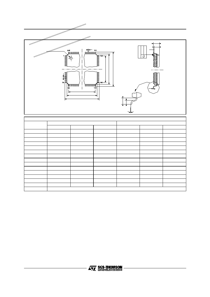
Dimensions
Ref.
Millimeters
Inches
Min.
Typ.
Max.
Min.
Typ.
Max.
A
4.10
0.0161
A1
0.25
0.010
A2
3.20
3.40
3.60
0.126
0.134
0.142
B
0.17
0.27
0.007
0.011
C
0.09
0.20
0.004
0.008
D
30.60
1.205
D1
28.00
1.102
D3
25.50
1.004
e
0.50
0.020
E
30.60
1.205
E1
28.00
1.102
E3
25.50
1.004
L
0.45
0.60
0.75
0.018
0.024
0.030
L1
1.30
0.051
K
0∞ (Min.), 7∞ (Max.)
Note : Exact shape of each corner is optional.
P
Q
F
P
2
0
8
.
T
B
L
This device is protected by US patent numbers 4631603, 4577216 and 4819098 and other intellectual property rights. The use of
Macrovision
TM
's copy protection technology in the device must be authorized by Macrovision
TM
and is intended for home and other limited
pay-per-view uses only, unless otherwise authorized in writing by Macrovision
TM
. Reverse engineering or disassembly is prohibited. Please
contact your nearest SGS-THOMSON Microelectronics sales office for more information.
PIN 1
IDENTIFICATION
E3
E1
E
D
3
D
1
D
B
e
A1
A
A2
L
K
C
L1
0
.
004
0
.
1
0
mm
S
e
a
t
i
ng
p
l
an
e
P
M
P
Q
F
2
0
8
.
E
P
S
IV - PACKAGE MECHANICAL DATA : 208 PINS - PLASTIC QUAD FLAT PACK
Information furnished is believed to be accurate and reliable. However, SGS-THOMSON Microelectronics assumes no responsibility
for the consequences of use of such information nor for any infringement of patents or other rights of third parties which may result
from its use. No licence is granted by implication or otherwise under any patent or patent rights of SGS-THOMSON Microelectronics.
Specifications mentioned in this publication are subject to change without notice. This publication supersedes and replaces all
information previously supplied. SGS-THOMSON Microelectronics products are not authorized for use as critical components in life
support decoders or systems without express written approval of SGS-THOMSON Microelectronics.
© 1997 SGS-THOMSON Microelectronics - All Rights Reserved
Purchase of I
2
C Components of SGS-THOMSON Microelectronics, conveys a license under the Philips
I
2
C Patent. Rights to use these components in a I
2
C system, is granted provided that the system conforms to
the I
2
C Standard Specifications as defined by Philips.
SGS-THOMSON Microelectronics GROUP OF COMPANIES
Australia - Brazil - Canada - China - France - Germany - Italy - Japan - Korea - Malaysia - Malta - Morocco
The Netherlands - Singapore - Spain - Sweden - Switzerland - Taiwan - Thailand - United Kingdom - U.S.A.
STi5500
11/11