 | –≠–ª–µ–∫—Ç—Ä–æ–Ω–Ω—ã–π –∫–æ–º–ø–æ–Ω–µ–Ω—Ç: STK13003 | –°–∫–∞—á–∞—Ç—å:  PDF PDF  ZIP ZIP |
STK13003
HIGH VOLTAGE FAST-SWITCHING
NPN POWER TRANSISTOR
s
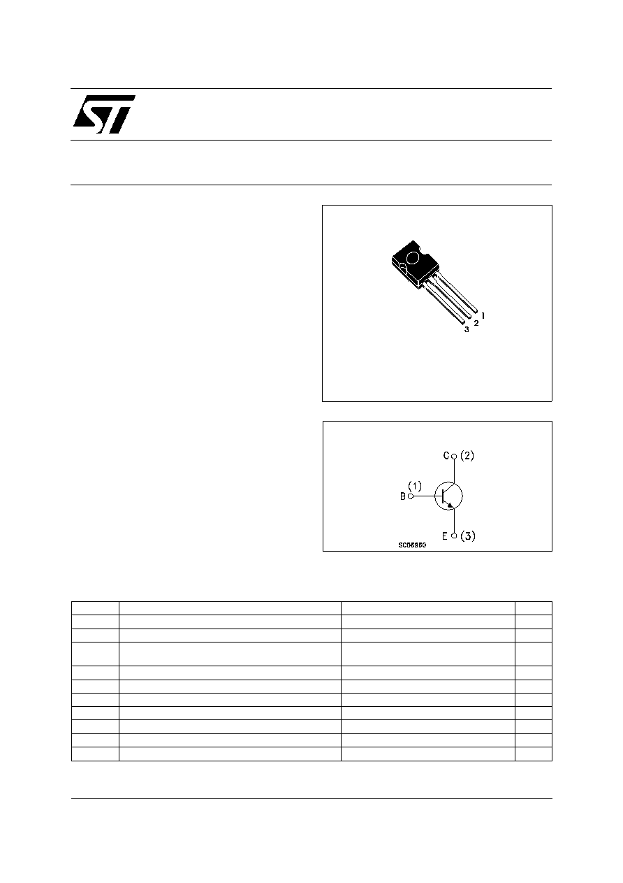
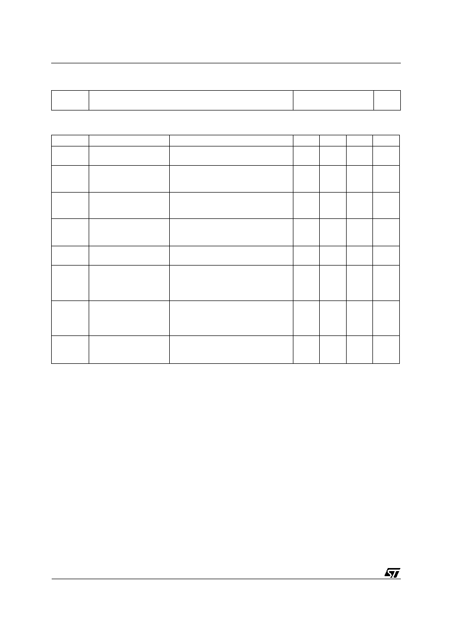
STK13003 IS REVERSE PINS OUT Vs
STANDARD SOT-82 PACKAGE
s
MEDIUM VOLTAGE CAPABILITY
s
LOW SPREAD OF DYNAMIC PARAMETERS
s
MINIMUM LOT-TO-LOT SPREAD FOR
RELIABLE OPERATION
s
VERY HIGH SWITCHING SPEED
APPLICATIONS:
s
ELECTRONIC BALLASTS FOR
FLUORESCENT LIGHTING
s
SWITCH MODE POWER SUPPLIES
DESCRIPTION
The device is manufactured using high voltage
Multi Epitaxial Planar technology for high
switching speeds and medium voltage capability.
It uses a Cellular Emitter structure with planar
edge termination to enhance switching speeds
while maintaining the wide RBSOA.
The device is designed for use in lighting
applications and low cost switch-mode power
supplies.
Æ
INTERNAL SCHEMATIC DIAGRAM
September 2001
ABSOLUTE MAXIMUM RATINGS
Symbol
Parameter
Value
Unit
V
CES
Collector-Emitter Voltage (V
BE
= 0)
700
V
V
CEO
Collector-Emitter Voltage (I
B
= 0)
400
V
V
EBO
Emitter-Base Voltage
(I
C
= 0, I
B
= 0.75 A, t
p
< 10
µ
s, T
j
< 150
o
C)
BV
EBO
V
I
C
Collector Current
1.5
A
I
CM
Collector Peak Current (t
p
< 5 ms)
3
A
I
B
Base Current
0.75
A
I
BM
Base Peak Current (t
p
< 5 ms)
1.5
A
P
tot
Total Dissipation at T
c
= 25
o
C
40
W
T
stg
Storage Temperature
-65 to 150
o
C
T
j
Max. Operating Junction Temperature
150
o
C
SOT-82
1/7
THERMAL DATA
R
thj-case
R
thj-amb
Thermal Resistance Junction-case Max
Thermal Resistance Junction-ambient Max
3.12
89
o
C/W
o
C/W
ELECTRICAL CHARACTERISTICS (T
case
= 25
o
C unless otherwise specified)
Symbol
Parameter
Test Conditions
Min.
Typ.
Max.
Unit
I
CEV
Collector Cut-off
Current (V
BE
= -1.5V)
V
CE
= 700V
V
CE
= 700V T
j
= 125
o
C
1
5
mA
mA
BV
EBO
Emitter-Base
Breakdown Voltage
(I
C
= 0)
I
E
= 10 mA
9
18
V
V
CEO(sus)
Collector-Emitter
Sustaining Voltage
(I
B
= 0)
I
C
= 10 mA
L = 25mH
400
V
V
CE(sat)
Collector-Emitter
Saturation Voltage
I
C
= 0.5 A I
B
= 0.1 A
I
C
= 1 A I
B
= 0.25 A
I
C
= 1.5 A I
B
= 0.5 A
0.5
1
3
V
V
V
V
BE(sat)
Base-Emitter
Saturation Voltage
I
C
= 0.5 A I
B
= 0.1 A
I
C
= 1 A I
B
= 0.25 A
1
1.2
V
V
h
FE
DC Current Gain
I
C
= 0.5 A V
CE
= 2 V
Group A
Group B
I
C
= 1 A V
CE
= 2 V
8
15
5
20
35
25
t
r
t
s
t
f
RESISTIVE LOAD
Rise Time
Storage Time
Fall Time
I
C
= 1 A V
CC
= 125 V
I
B1
= 0.2 A I
B2
= -0.2 A
T
p
= 25
µ
s
1
4
0.7
µ
s
µ
s
µ
s
t
s
INDUCTIVE LOAD
Storage Time
I
C
= 1 A I
B1
= 0.2 A
V
BE
= -5 V L = 50 mH
V
clamp
= 300 V
0.8
µ
s
Pulsed: Pulse duration = 300
µ
s, duty cycle = 1.5 %
Note : Product is pre-selected in DC current gain (GROUP A and GROUP B). STMicroelectronics reserves the right to ship either groups
according to production availability. Please contact your nearest STMicroelectronics sales office for delivery details.
STK13003
2/7
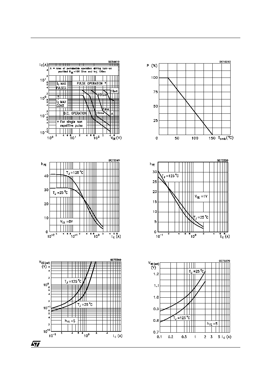
Safe Operating Areas
DC Current Gain
Collector Emitter Saturation Voltage
Derating Curve
DC Current Gain
Base Emitter Saturation Voltage
STK13003
3/7
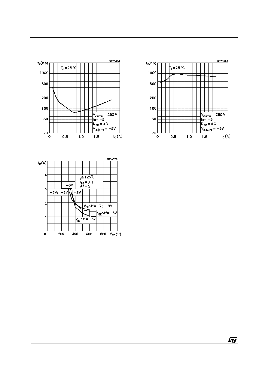
Inductive Load Fall Time
Inductive Load Storage Time
Reverse Biased SOA
STK13003
4/7
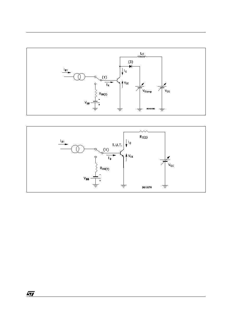
Figure 1: Inductive Load Switching Test Circuits.
Figure 2: Resistive Load Switching Test Circuits.
1) Fast electronic switch
2) Non-inductive Resistor
3) Fast recovery rectifier
1) Fast electronic switch
2) Non-inductive Resistor
STK13003
5/7