1/9
June 2005
STL20NM20N
N-CHANNEL 200V - 0.088
- 20A PowerFLATTM
ULTRA LOW GATE CHARGE MDmeshTM II MOSFET
Table 1: General Features
s
WORLDWIDE LOWEST GATE CHARGE
s
TYPICAL R
DS
(on) = 0.088
s
IMPROVED DIE-TO-FOOTPRINT RATIO
s
VERY LOW PROFILE PACKAGE (1mm MAX)
s
VERY LOW THERMAL RESISTANCE
s
LOW GATE RESISTANCE
s
LOW INPUT CAPACITANCE
s
HIGH dv/dt and AVALANCHE CAPABILITIES
DESCRIPTION
This 200V MOSFET with a new advanced layout
brings all unique advantages of MDmesh technol-
ogy to lower voltages. The device exhibits world-
wide lowest gate charge for any given on-
resistance.Its use is therefore ideal as primary
switch in isolated DC-DC converters for Telecom
and Computer applications.Used in combination
with secondary-side low-voltage STripFET
TM
prod-
ucts, it contributes to reducing losses and boosting
efficiency.The new PowerFLATTM package allows
a significant reduction in board space without com-
promising performance.
APPLICATIONS
The MDmesh
TM
family is very suitable for increas-
ing power density allowing system miniaturization
and higher efficiencies
Table 2: Order Codes
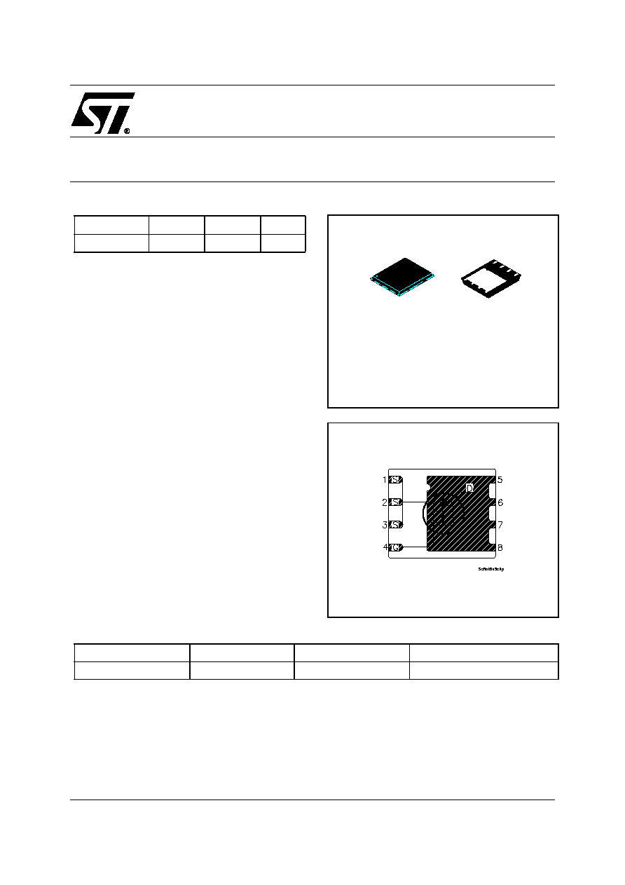
Figure 1: Package
Figure 2: Internal Schematic Diagram
TYPE
V
DSS
R
DS(on)
I
D
STL20NM20N
200 V
< 0.105
20 A
PowerFlat (6x5)
(Chip Scale Package)
SALES TYPE
MARKING
PACKAGE
PACKAGING
STL20NM20N
L20NM20N
PowerFLATTM(6x5)
TAPE & REEL
Rev. 3
STL20NM20N
2/9
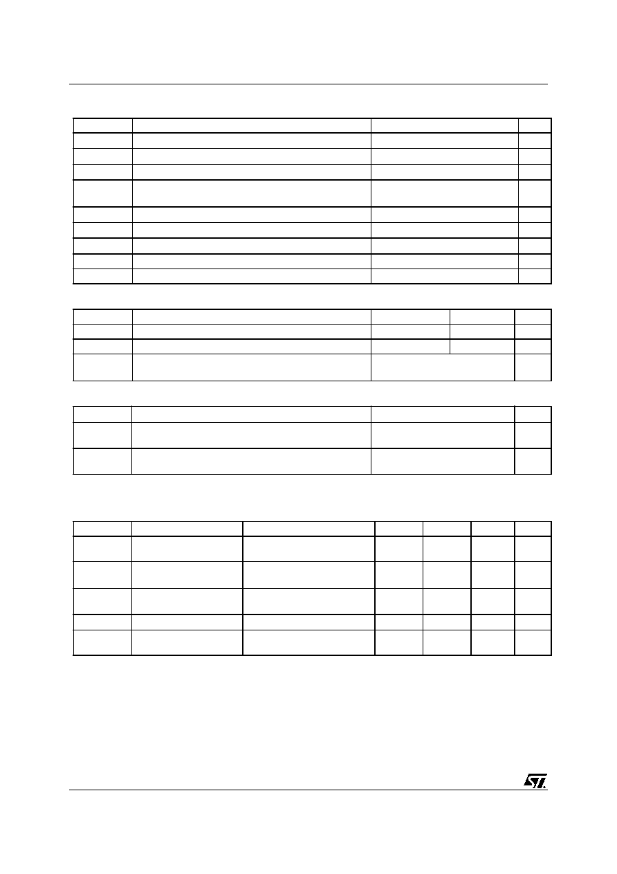
Table 3: Absolute Maximum ratings
Table 4: Thermal Data
Table 5: Avalanche Characteristics
ELECTRICAL CHARACTERISTICS (T
CASE
=25∞C UNLESS OTHERWISE SPECIFIED)
Table 6: On/Off
Symbol
Parameter
Value
Unit
V
DS
Drain-source Voltage (V
GS
= 0)
200
V
V
DGR
Drain-gate Voltage (R
GS
= 20 k
)
200
V
V
GS
Gate- source Voltage
± 30
V
I
D
(1)
Drain Current (continuous) at T
C
= 25∞C (Steady State)
Drain Current (continuous) at T
C
= 100∞C
20
12.3
A
A
I
DM
(3)
Drain Current (pulsed)
80
A
P
TOT
(2)
Total Dissipation at T
C
= 25∞C (Steady State)
2.5
W
P
TOT
(1)
Total Dissipation at T
C
= 25∞C (Steady State)
80
W
Derating Factor (2)
0.02
W/∞C
dv/dt (4)
Peak Diode Recovery voltage slope
10
V/ns
Symbol
Parameter
Typ.
Max.
Unit
Rthj-c
Thermal Resistance Junction-case
1.56
∞C/W
Rthj-pcb (2)
Thermal Resistance Junction-pcb
35
50
∞C/W
T
j
T
stg
Max. Operating Junction Temperature
Storage Temperature
-55 to 150
∞C
Symbol
Parameter
Max. Value
Unit
I
AS
Avalanche Current, Repetitive or Not-Repetitive
(pulse width limited by T
j
max)
20
A
E
AS
Single Pulse Avalanche Energy
(starting T
j
= 25 ∞C, I
D
= I
AR
, V
DD
= 35 V)
380
mJ
Symbol
Parameter
Test Conditions
Min.
Typ.
Max.
Unit
V
(BR)DSS
Drain-source
Breakdown Voltage
I
D
= 1 mA, V
GS
= 0
200
V
I
DSS
Zero Gate Voltage
Drain Current (V
GS
= 0)
V
DS
= Max Rating
V
DS
= Max Rating, T
C
= 125 ∞C
1
10
µA
µA
I
GSS
Gate-body Leakage
Current (V
DS
= 0)
V
GS
= ± 30 V
±100
nA
V
GS(th)
Gate Threshold Voltage
V
DS
= V
GS
, I
D
= 250 µA
3
4
5
V
R
Ds(on)
Static Drain-source On
Resistance
V
GS
= 10V, I
D
= 10 A
0.088
0.105
3/9
STL20NM20N
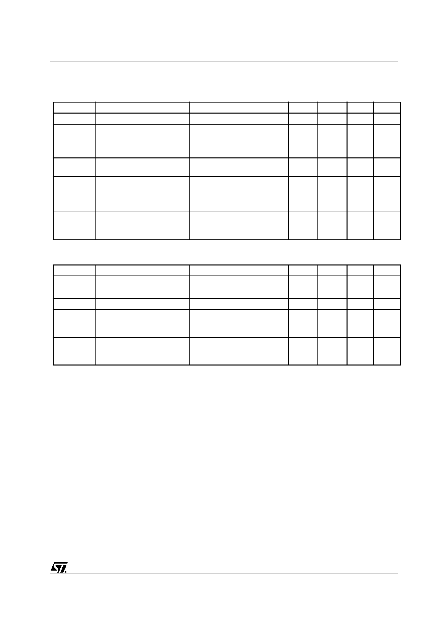
ELECTRICAL CHARACTERISTICS (CONTINUED)
Table 7: Dynamic
(*) C
oss eq.
is defined as a constant equivalent capacitance giving the same charging time as C
oss
when V
DS
increases from 0 to 80% V
DSS
Table 8: Source Drain Diode
Note: 1. The value is rated according to R
thj-c
.
2. When Mounted on FR-4 Board of 1inch
2
, 2 oz Cu
3. Pulse width limited by safe operating area
4. I
SD
20A, di/dt
400A/µs, V
DD
V
(BR)DSS
5. Pulsed: Pulse duration = 300 µs, duty cycle 1.5 %
Symbol
Parameter
Test Conditions
Min.
Typ.
Max.
Unit
g
fs
(5)
Forward Transconductance
V
DS
= 15 V
,
I
D
= 10 A
8
S
C
iss
C
oss
C
rss
Input Capacitance
Output Capacitance
Reverse Transfer
Capacitance
V
DS
= 25 V, f = 1 MHz, V
GS
= 0
800
330
130
pF
pF
pF
C
oss eq.
(*)
Equivalent Output
Capacitance
V
GS
= 0V, V
DS
= 0V to 160 V
225
pF
t
d(on)
t
r
t
d(off)
t
f
Turn-on Delay Time
Rise Time
Turn-off Delay Time
Fall Time
V
DD
= 100 V, I
D
= 10 A
R
G
= 4.7
V
GS
= 10 V
(see Figure 16)
40
15
40
11
ns
ns
ns
ns
Q
g
Q
gs
Q
gd
Total Gate Charge
Gate-Source Charge
Gate-Drain Charge
V
DD
= 160 V, I
D
= 20 A,
V
GS
= 10 V
(see Figure 19)
32
6
25
50
nC
nC
nC
Symbol
Parameter
Test Conditions
Min.
Typ.
Max.
Unit
I
SD
Source-drain Current
20
A
I
SDM
(3)
Source-drain Current (pulsed)
80
A
V
SD
(5)
Forward On Voltage
I
SD
= 20 A, V
GS
= 0
1.3
V
t
rr
Q
rr
I
RRM
Reverse Recovery Time
Reverse Recovery Charge
Reverse Recovery Current
I
SD
= 20 A, di/dt = 100 A/µs,
V
DD
= 100 V, T
j
= 25∞C
(see Figure 17)
160
960
128
ns
nC
A
t
rr
Q
rr
I
RRM
Reverse Recovery Time
Reverse Recovery Charge
Reverse Recovery Current
I
SD
= 20 A, di/dt = 100 A/µs,
V
DD
= 100 V, T
j
= 150∞C
(see Figure 17)
225
1642
15
ns
nC
A
STL20NM20N
4/9
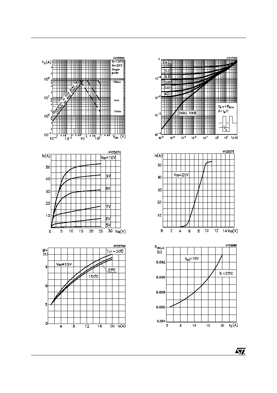
Figure 3: Safe Operating Area
Figure 4: Output Characteristics
Figure 5: Transconductance
Figure 6: Thermal Impedance
Figure 7: Transfer Characteristics
Figure 8: Static Drain-source On Resistance
5/9
STL20NM20N
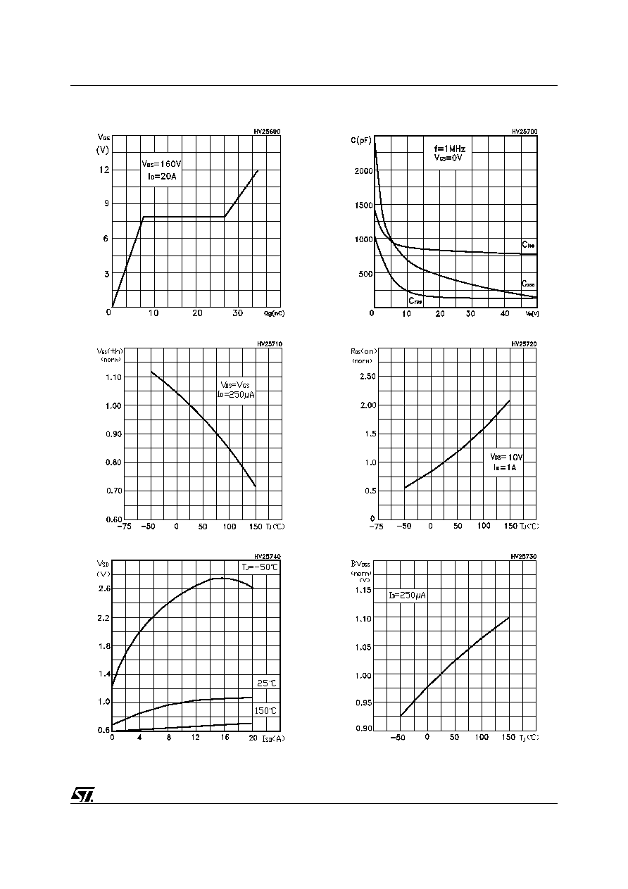
Figure 9: Gate Charge vs Gate-source Voltage
Figure 10: Normalized Gate Thereshold Volt-
age vs Temperature
Figure 11: Source-Drain Diode Forward Char-
acteristics
Figure 12: Capacitance Variations
Figure 13: Normalized On Resistance vs Tem-
perature
Figure 14: Normalized BVdss vs Temperature