1/6
PRELIMINARY DATA
November 2002
STL28NF3LL
N-CHANNEL 30V - 0.0055
- 28A PowerFLATTM
LOW GATE CHARGE STripFETTM MOSFET
(1) Starting T
j
= 25∞C, I
D
= 14A, V
DD
= 18V
s
TYPICAL R
DS
(on) = 0.0055
s
IMPROVED DIE-TO-FOOTPRINT RATIO
s
VERY LOW PROFILE PACKAGE
DESCRIPTION
This Power MOSFET is the second generation of
STMicroelectronics unique "STripFETTM" technolo-
gy. The resulting transistor shows extremely low on-
resistance and minimal gate charge. The new Pow-
erFLATTM package allows a significant reduction in
board space without compromising performance.
APPLICATIONS
s
DC-DC CONVERTERS
ABSOLUTE MAXIMUM RATINGS
(
q
) Pulse width limited by safe operating area
(#) Limited by Wire Bonding
TYPE
V
DSS
R
DS(on)
I
D
STL28NF3LL
30 V
< 0.0065
28 A
Symbol
Parameter
Value
Unit
V
DS
Drain-source Voltage (V
GS
= 0)
30
V
V
DGR
Drain-gate Voltage (R
GS
= 20 k
)
30
V
V
GS
Gate- source Voltage
± 16
V
I
D
(#)
Drain Current (continuos) at T
C
= 25∞C
Drain Current (continuos) at T
C
= 100∞C
28
17.5
A
A
I
DM
( )
Drain Current (pulsed)
112
A
P
TOT
Total Dissipation at T
C
= 25∞C
80
W
Derating Factor
0.64
W/∞C
E
AS
(1)
Single Pulse Avalanche Energy
2
J
T
stg
Storage Temperature
≠55 to 150
∞C
T
j
Max. Operating Junction Temperature
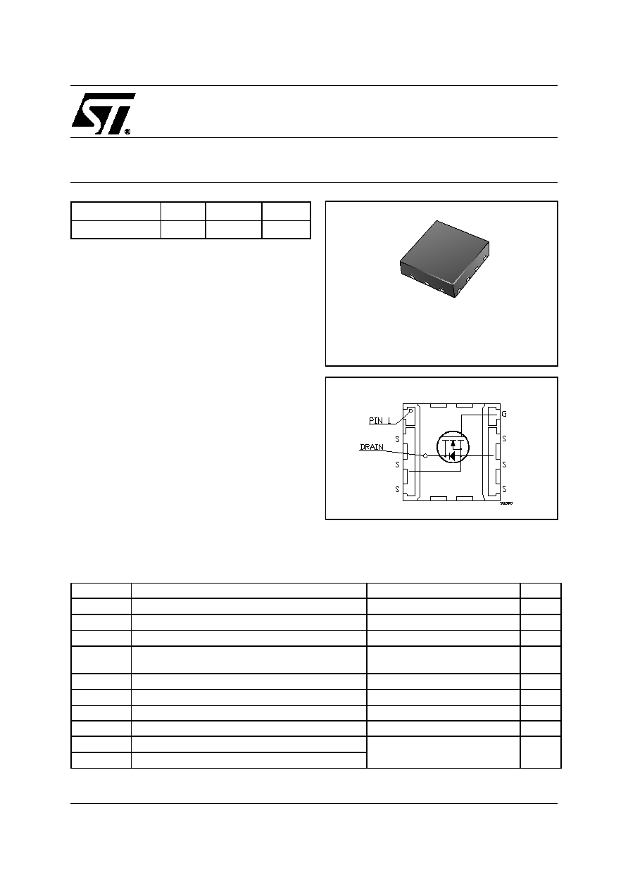
PowerFLATTM(5x5)
(Chip Scale Package)
INTERNAL SCHEMATIC DIAGRAM
STL28NF3LL
2/6
THERMAL DATA
(*) When mounted on 1inch≤ FR4 Board, 2oz of Cu, t
10 sec.
ELECTRICAL CHARACTERISTICS (TCASE = 25 ∞C UNLESS OTHERWISE SPECIFIED)
OFF
ON (1)
DYNAMIC
Rthj-case
Thermal Resistance Junction-case Max
1.56
∞C/W
Rthj-pcb (#)
Thermal Resistance Junction-ambient Max
31.2
∞C/W
Symbol
Parameter
Test Conditions
Min.
Typ.
Max.
Unit
V
(BR)DSS
Drain-source
Breakdown Voltage
I
D
= 250 µA, V
GS
= 0
30
V
I
DSS
Zero Gate Voltage
Drain Current (V
GS
= 0)
V
DS
= Max Rating
1
µA
V
DS
= Max Rating, T
C
= 125 ∞C
10
µA
I
GSS
Gate-body Leakage
Current (V
DS
= 0)
V
GS
= ± 16V
±100
nA
Symbol
Parameter
Test Conditions
Min.
Typ.
Max.
Unit
V
GS(th)
Gate Threshold Voltage
V
DS
= V
GS
, I
D
= 250µA
1
V
R
DS(on)
Static Drain-source On
Resistance
V
GS
= 10 V, I
D
= 14 A
0.0055
0.0065
V
GS
= 4.5 V, I
D
= 14A
0.0065
0.0095
Symbol
Parameter
Test Conditions
Min.
Typ.
Max.
Unit
g
fs
(1)
Forward Transconductance
V
DS
= 15 V
,
I
D
= 14 A
32
S
C
iss
Input Capacitance
V
DS
= 25 V, f = 1 MHz, V
GS
= 0
2780
pF
C
oss
Output Capacitance
890
pF
C
rss
Reverse Transfer
Capacitance
195
pF
3/6
STL28NF3LL
ELECTRICAL CHARACTERISTICS (CONTINUED)
SWITCHING ON
SWITCHING OFF
SOURCE DRAIN DIODE
Note: 1. Pulsed: Pulse duration = 300 µs, duty cycle 1.5 %.
2. Pulse width limited by safe operating area.
Symbol
Parameter
Test Conditions
Min.
Typ.
Max.
Unit
t
d(on)
Turn-on Delay Time
V
DD
= 15 V, I
D
= 14 A
R
G
= 4.7
V
GS
= 4.5V
(see test circuit, Figure 3)
25
ns
t
r
Rise Time
82
ns
Q
g
Q
gs
Q
gd
Total Gate Charge
Gate-Source Charge
Gate-Drain Charge
V
DD
= 15 V, I
D
= 28 A,
V
GS
= 5 V
32
13
18
43
nC
nC
nC
Symbol
Parameter
Test Conditions
Min.
Typ.
Max.
Unit
t
d(off)
t
f
Turn-off-Delay Time
Fall Time
V
DD
= 15 V, I
D
= 14 A,
R
G
= 4.7
,
V
GS
= 4.5 V
(see test circuit, Figure 3)
42
35
ns
ns
Symbol
Parameter
Test Conditions
Min.
Typ.
Max.
Unit
I
SD
Source-drain Current
28
A
I
SDM
(2)
Source-drain Current (pulsed)
112
A
V
SD
(1)
Forward On Voltage
I
SD
= 28 A, V
GS
= 0
1.2
V
t
rr
Q
rr
I
RRM
Reverse Recovery Time
Reverse Recovery
ChargeReverse Recovery
Current
I
SD
= 28 A, di/dt = 100A/µs,
V
DD
= 25 V, T
j
= 150∞C
(see test circuit, Figure 5)
50
82
3.3
ns
nC
A
STL28NF3LL
4/6
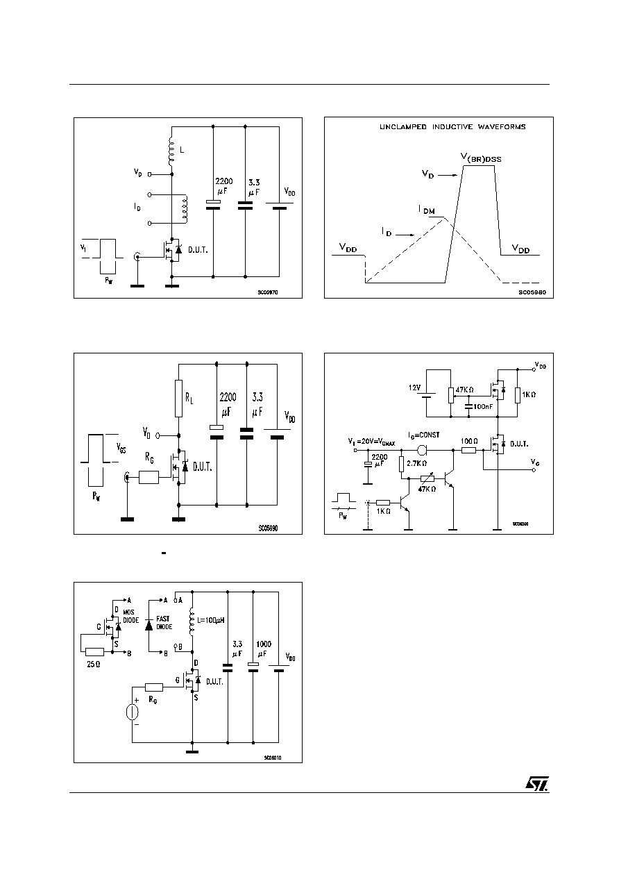
Fig. 5: Test Circuit For Inductive Load Switching
And Diode Recovery Times
Fig. 4: Gate Charge test Circuit
Fig. 2: Unclamped Inductive Waveform
Fig. 1: Unclamped Inductive Load Test Circuit
Fig. 3: Switching Times Test Circuit For
Resistive Load

STL28NF3LL
5/6
DIM.
mm.
inch
MIN.
TYP
MAX.
MIN.
TYP.
MAX.
A
0.90
1.00
0.035
0.039
A1
0.02
0.05
0.001
0.002
b
0.43
0.51
0.58
0.017
0.020
0.023
c
0.33
0.41
0.48
0.013
0.016
0.019
D
5.00
0.197
E
5.00
0.197
E2
3.10
3.18
3.25
0.122
0.125
0.128
e
1.27
0.050
PowerFLATTM(5x5) MECHANICAL DATA