1/6
July 2005
n
MEDIUM
VOLTAGE
CAPABILITY
n
LOW SPREAD OF DYNAMIC PARAMETERS
n
MINIMUM LOT-TO-LOT SPREAD FOR
RELIABLE OPERATION
n
VERY HIGH SWITCHING SPEED
APPLICATIONS
n
ELECTRONIC BALLASTS FOR
FLUORESCENT LIGHTING
DESCRIPTION
The device is manufactured using high voltage
Multi-Epitaxial Planar technology for high
switching speeds and medium voltage capability.
It uses a Cellular Emitter structure with planar
edge termination to enhance switching speeds
while maintaining the wide RBSOA.
The STL series is designed for use in Compact
Fluorescent Lamps.
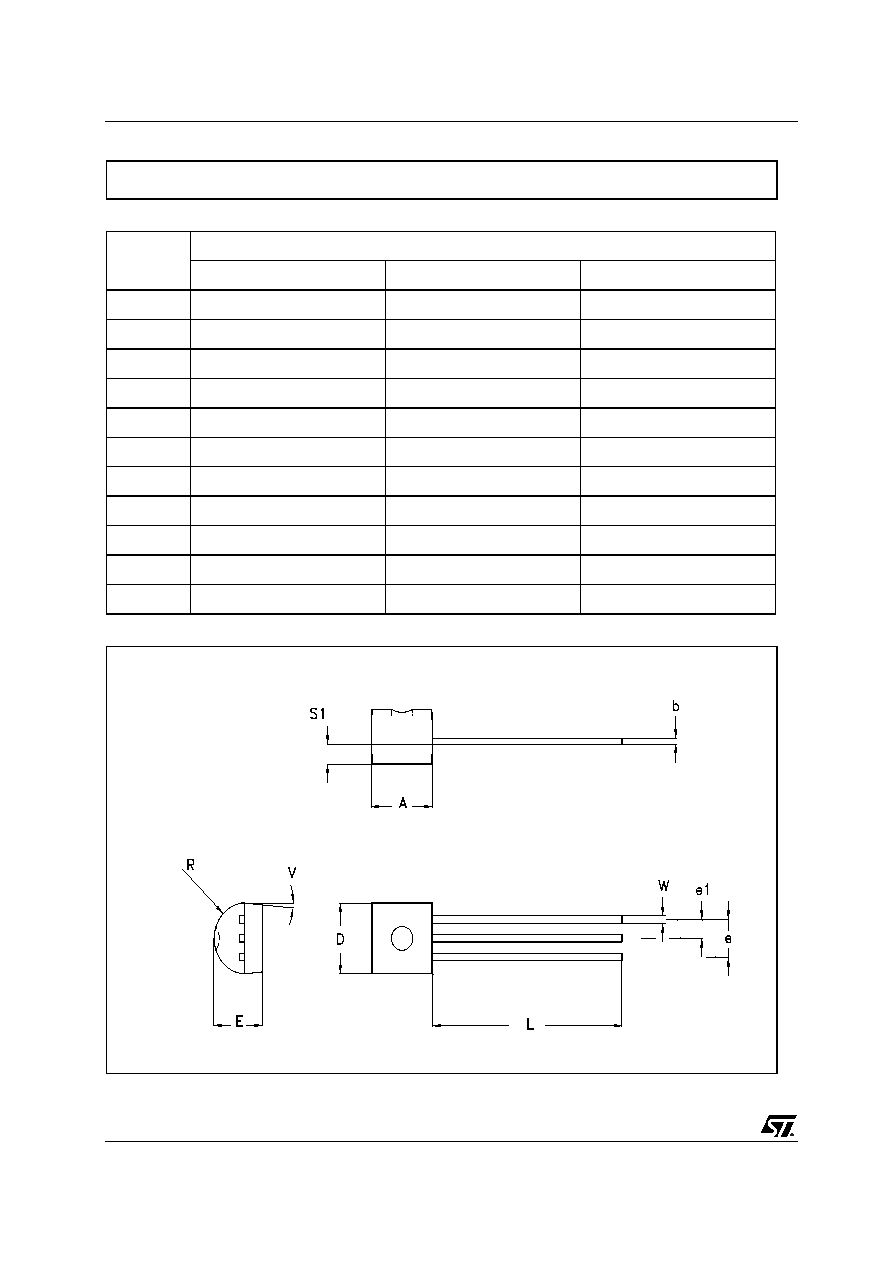
Figure 1: Package
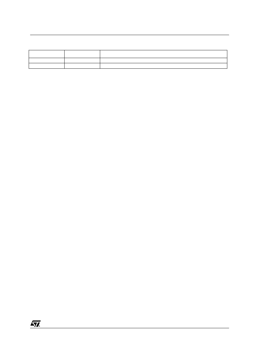
Figure 2: Internal Schematic Diagram
Table 1: Order Codes
# See:note on page 2
TO-92
Part Number
Marking
Package
Packaging
STL72
L72 L
or (#)
L72 H
TO-92
Bulk
STL72
MEDIUM VOLTAGE FAST-SWITCHING
NPN POWER TRANSISTOR
Rev. 2

STL72
2/6
Table 2: Absolute Maximum Ratings
Table 3: Thermal Data
Table 4: Electrical Characteristics (T
case
= 25
o
C unless otherwise specified)
* Pulsed: Pulsed duration = 300 ms, duty cycle
1.5
%.
#
The product is pre-selected in DC current gain (Group L and Group H). STMicroelectronics reserves the right to ship either groups accord-
ing to production availability. Please contact your nearest STMicrolectronics sales office for delivery datails.
Symbol
Parameter
Value
Unit
V
CES
Collector-Emitter Voltage (V
BE
= 0)
700
V
V
CEO
Collector-Emitter Voltage (I
B
= 0)
400
V
V
EBO
Emitter-Base Voltage (I
C
= 0)
9
V
I
C
Collector Current
1
A
I
CM
Collector Peak Current (t
p
< 5ms)
2
A
I
B
Base Current
0.5
A
I
BM
Base Peak Current (t
p
< 5ms)
1
A
P
tot
Total Dissipation at T
C
= 25
o
C
1
W
T
stg
Storage Temperature
-65 to 150
°C
T
J
Max. Operating Junction Temperature
150
°C
R
thj-amb
Thermal Resistance Junction-Ambient Max
120
o
C/W
Symbol
Parameter
Test Conditions
Min.
Typ.
Max.
Unit
I
CEV
Collector Cut-off Current
(V
BE
= -1.5 V)
V
CE
= 700 V
V
CE
= 700 V T
j
= 125
o
C
1
5
mA
mA
I
EBO
Emitter-Cut-off Current
(I
C
= 0 )
V
EB
= 9 V
1
mA
V
CEO(sus)
* Collector-Emitter
Sustaining Voltage
(I
B
= 0 )
I
C
= 1 mA L = 25 mH
400
V
V
CE(sat)
*
Collector-Emitter
Saturation Voltage
I
C
= 0.2 A I
B
= 40 mA
I
C
= 0.4 A I
B
= 80 mA
0.15
0.25
0.4
0.5
V
V
V
BE(sat)
*
Base-Emitter Saturation
Voltage
I
C
= 0.4 A I
B
= 80 mA
0.95
1.1
V
h
FE
DC Current Gain #
I
C
= 0.4 A V
CE
= 5 V
Group L
Group H
I
C
= 1 A V
CE
= 10 V
10
15
5
16
23
15
t
f
INDUCTIVE LOAD
Fall Time
I
C
= 0.25 V
Clamp
= 300 V
I
B1
= -I
B2
= 50 mA L = 3mH
(see figure 3)
0.3
µs
STL72
3/6
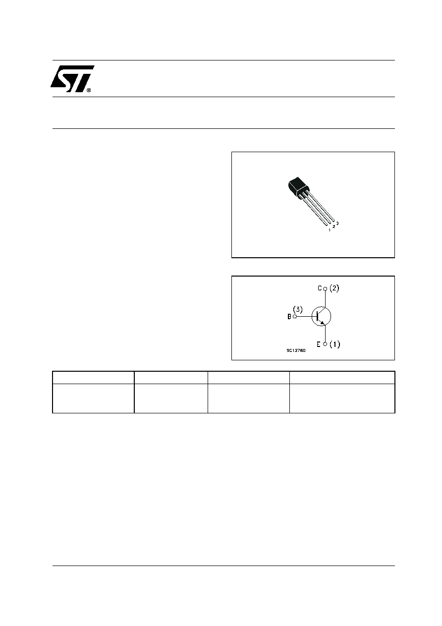
Figure 3: Inductive Load Switching Test Circuit
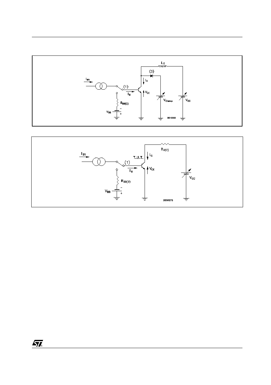
Figure 4: Restistive Load Switching Test Circuit
1) Fast electronic switch
2) Non-inductive Resistor
3) Fast recovery rectifier
1) Fast electronic switch
2) Non-inductive Resistor