 | –≠–ª–µ–∫—Ç—Ä–æ–Ω–Ω—ã–π –∫–æ–º–ø–æ–Ω–µ–Ω—Ç: STL9NK30Z | –°–∫–∞—á–∞—Ç—å:  PDF PDF  ZIP ZIP |
1/8
August 2002
STL9NK30Z
N-CHANNEL 300V - 0.36
- 9A PowerFLATTM
Zener-Protected SuperMESHTMPower MOSFET
s
TYPICAL R
DS
(on) = 0.36
s
EXTREMELY HIGH dv/dt CAPABILITY
s
IMPROVED ESD CAPABILITY
s
100% AVALANCHE RATED
s
GATE CHARGE MINIMIZED
s
VERY LOW INTRINSIC CAPACITANCES
s
VERY GOOD MANUFACTURING
REPEATIBILITY
DESCRIPTION
The SuperMESHTM series is obtained through an
extreme optimization of ST's well established strip-
based PowerMESHTM layout. In addition to pushing
on-resistance significantly down, special care is tak-
en to ensure a very good dv/dt capability for the
most demanding applications. Such series comple-
ments ST full range of high voltage MOSFETs in-
cluding revolutionary MDmeshTM products.
APPLICATIONS
s
LIGHTING
s
IDEAL FOR OFF-LINE POWER SUPPLIES,
ADAPTORS AND PFC
ORDERING INFORMATION
TYPE
V
DSS
R
DS(on)
I
D
(1)
Pw (1)
STL9NK30Z
300 V
< 0.4
9 A
75 W
SALES TYPE
MARKING
PACKAGE
PACKAGING
STL9NK30Z
L9NK30Z
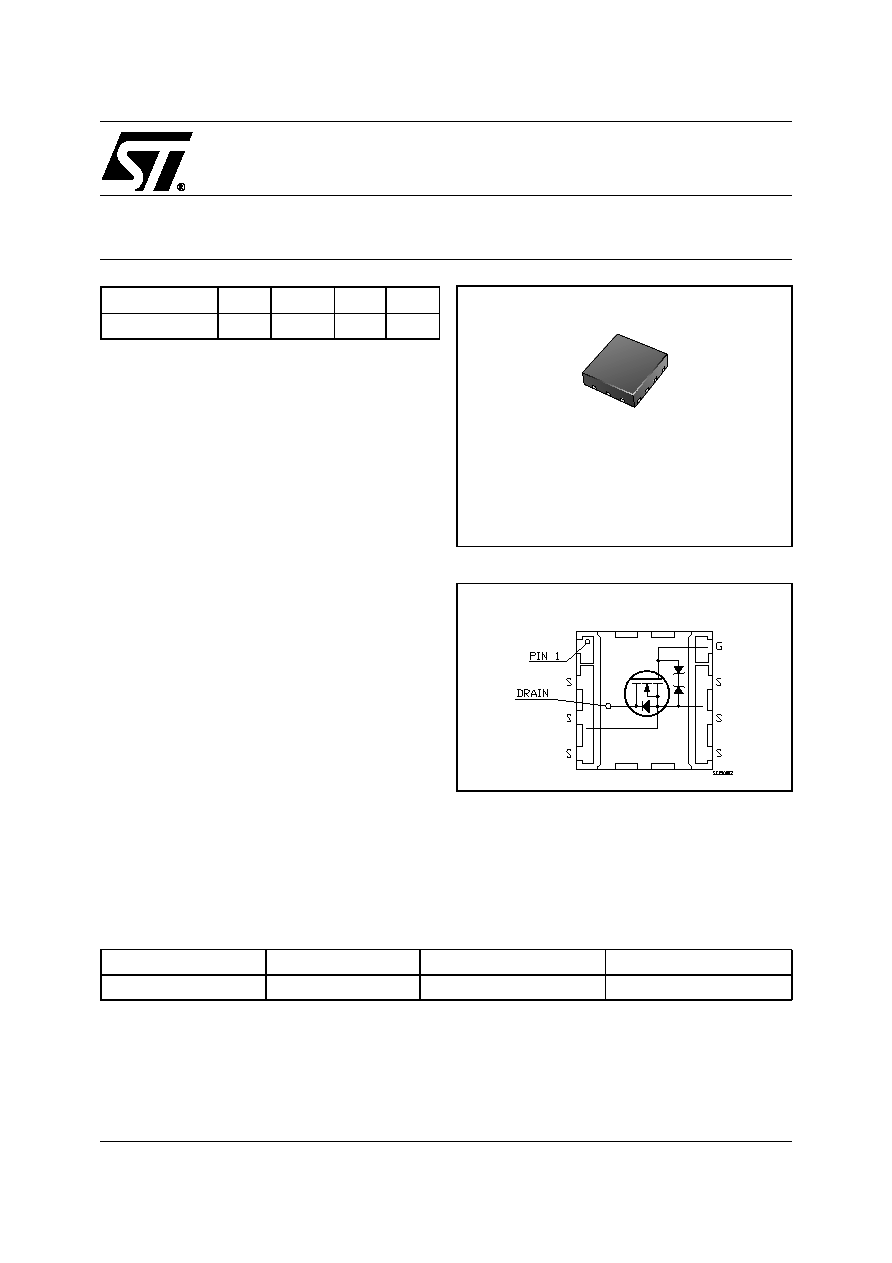
PowerFLATTM (5x5)
TAPE & REEL
PowerFLATTM(5x5)
(Chip Scale Package)
INTERNAL SCHEMATIC DIAGRAM
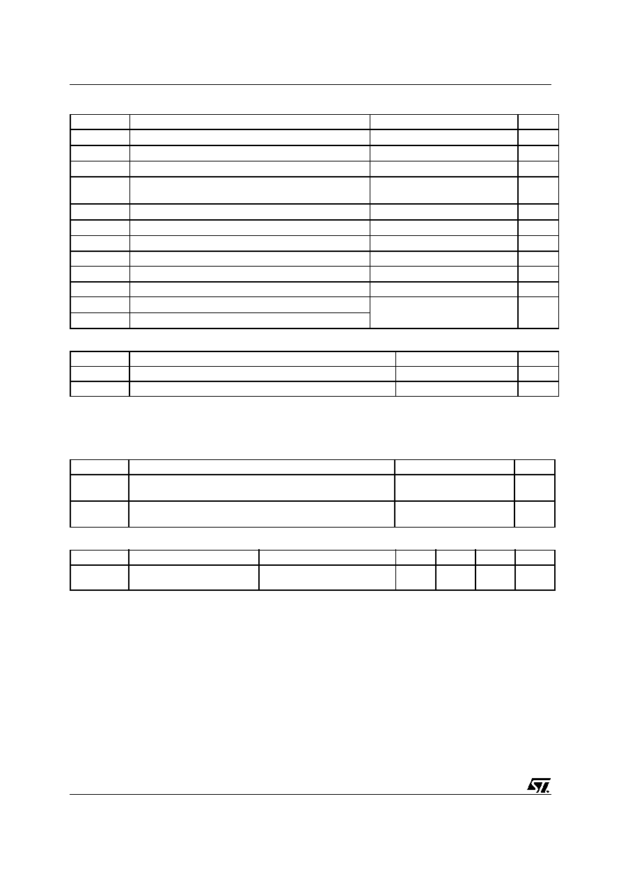
STL9NK30Z
2/8
ABSOLUTE MAXIMUM RATINGS
THERMAL DATA
Note: 1. The value is rated according to R
thj-F
.
2. When Mounted on FR-4 Board of 1inch
2
, 2 oz Cu
3. Pulse width limited by safe operating area
4. I
SD
< 9A, di/dt<300A/µs, V
DD
<V
(BR)DSS
, T
J
<T
JMAX
AVALANCHE CHARACTERISTICS
GATE-SOURCE ZENER DIODE
PROTECTION FEATURES OF GATE-TO-SOURCE ZENER DIODES
The built-in back-to-back Zener diodes have specifically been designed to enhance not only the device's
ESD capability, but also to make them safely absorb possible voltage transients that may occasionally be
applied from gate to source. In this respect the Zener voltage is appropriate to achieve an efficient and
cost-effective intervention to protect the device's integrity. These integrated Zener diodes thus avoid the
usage of external components.
Symbol
Parameter
Value
Unit
V
DS
Drain-source Voltage (V
GS
= 0)
300
V
V
DGR
Drain-gate Voltage (R
GS
= 20 k
)
300
V
V
GS
Gate- source Voltage
± 30
V
I
D
(2)
Drain Current (continuous) at T
C
= 25∞C (Steady State)
Drain Current (continuous) at T
C
= 100∞C
9
5.6
A
A
I
DM
(2)
Drain Current (pulsed)
36
A
P
TOT
(2)
Total Dissipation at T
C
= 25∞C (Steady State)
2.5
W
P
TOT
(1)
Total Dissipation at T
C
= 25∞C (Steady State)
75
W
Derating Factor (2)
0.6
W/∞C
V
ESD(G-S)
Gate source ESD(HBM-C=100pF, R=1.5K
)
3000
V/ns
dv/dt (4)
Peak Diode Recovery voltage slope
4.5
V/ns
T
stg
Storage Temperature
≠55 to 150
∞C
T
j
Max. Operating Junction Temperature
Symbol
Parameter
Max.
Unit
Rthj-F
Thermal Resistance Junction-Foot (Drain)
1.6
∞C/W
Rthj-amb (2)
Thermal Resistance Junction-ambient
50
∞C/W
Symbol
Parameter
Max Value
Unit
I
AR
Avalanche Current, Repetitive or Not-Repetitive
(pulse width limited by T
j
max)
9
A
E
AS
Single Pulse Avalanche Energy
(starting T
j
= 25 ∞C, I
D
= I
AR
, V
DD
= 50 V)
155
mJ
Symbol
Parameter
Test Conditions
Min.
Typ.
Max.
Unit
BV
GSO
Gate-Source Breakdown
Voltage
Igs=± 1mA (Open Drain)
30
V
3/8
STL9NK30Z
ELECTRICAL CHARACTERISTICS (TCASE =25∞C UNLESS OTHERWISE SPECIFIED)
ON/OFF
DYNAMIC
SWITCHING
SOURCE DRAIN DIODE
Note: 1. Pulsed: Pulse duration = 300 µs, duty cycle 1.5 %.
2. Pulse width limited by safe operating area.
3. C
oss eq.
is defined as a constant equivalent capacitance giving the same charging time as C
oss
when V
DS
increases from 0 to 80%
V
DSS
.
Symbol
Parameter
Test Conditions
Min.
Typ.
Max.
Unit
V
(BR)DSS
Drain-source
Breakdown Voltage
I
D
= 1 mA, V
GS
= 0
300
V
I
DSS
Zero Gate Voltage
Drain Current (V
GS
= 0)
V
DS
= Max Rating
V
DS
= Max Rating, T
C
= 125 ∞C
1
50
µA
µA
I
GSS
Gate-body Leakage
Current (V
DS
= 0)
V
GS
= ± 20V
±10
µA
V
GS(th)
Gate Threshold Voltage
V
DS
= V
GS
, I
D
= 50µA
3
3.75
4.5
V
R
DS(on)
Static Drain-source On
Resistance
V
GS
= 10V, I
D
= 4.5 A
0.36
0.4
Symbol
Parameter
Test Conditions
Min.
Typ.
Max.
Unit
g
fs
(1)
Forward Transconductance
V
DS
= 10 V
,
I
D
= 4.5 A
5.4
S
C
iss
C
oss
C
rss
Input Capacitance
Output Capacitance
Reverse Transfer
Capacitance
V
DS
= 25V, f = 1 MHz, V
GS
= 0
670
125
28
pF
pF
pF
C
oss eq.
(3)
Equivalent Output
Capacitance
V
GS
= 0V, V
DS
= 0V to 440 V
70
pF
R
G
Gate Input Resistance
f=1 MHz Gate DC Bias = 0
Test Signal Level = 20mV
Open Drain
3.6
Symbol
Parameter
Test Conditions
Min.
Typ.
Max.
Unit
t
d(on)
t
r
t
d(off)
t
f
Turn-on Delay Time
Rise time
Turn-off Delay Time
Fall Time
V
DD
= 150 V, I
D
= 4.5 A
R
G
= 4.7
V
GS
= 10 V
(Resistive Load see, Figure 3)
16
20
36
10
ns
ns
ns
ns
Q
g
Q
gs
Q
gd
Total Gate Charge
Gate-Source Charge
Gate-Drain Charge
V
DD
= 240V, I
D
= 9 A,
V
GS
= 10V
25
5.5
13.4
35
nC
nC
nC
Symbol
Parameter
Test Conditions
Min.
Typ.
Max.
Unit
I
SD
I
SDM
(2)
Source-drain Current
Source-drain Current (pulsed)
9
36
A
A
V
SD
(1)
Forward On Voltage
I
SD
= 9 A, V
GS
= 0
1.6
V
t
rr
Q
rr
I
RRM
Reverse Recovery Time
Reverse Recovery Charge
Reverse Recovery Current
I
SD
= 9 A, di/dt = 100A/µs
V
DD
= 40V, T
j
= 150∞C
(see test circuit, Figure 5)
165
0.9
11.2
ns
µC
A
STL9NK30Z
4/8
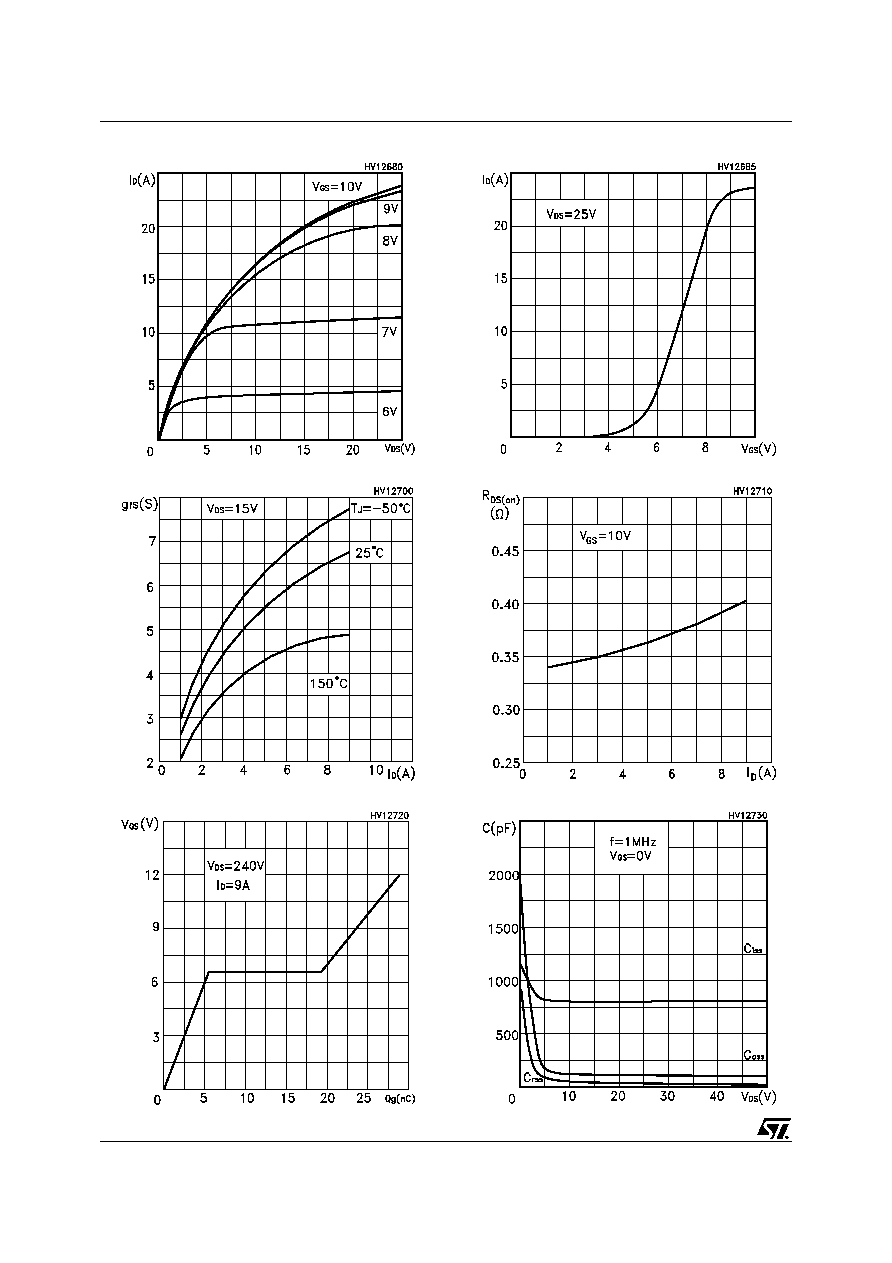
Capacitance Variations
Gate Charge vs Gate-source Voltage
Static Drain-source On Resistance
Transfer Characteristics
Output Characteristics
Transconductance
5/8
STL9NK30Z
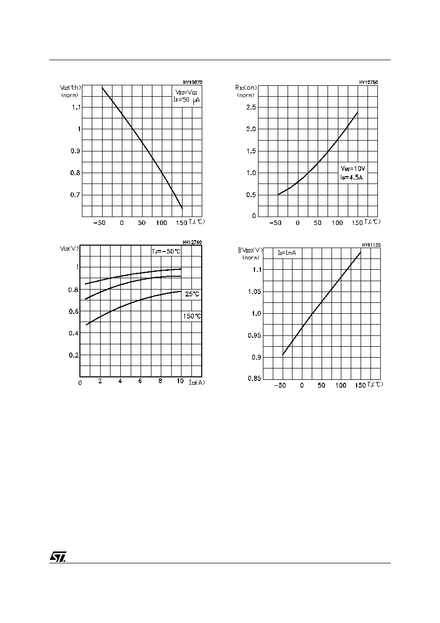
Normalized Gate Thereshold Voltage vs Temp.
Source-drain Diode Forward Characteristics
Normalized On Resistance vs Temperature
Normalized BVDSS vs Temperature