 | –≠–ª–µ–∫—Ç—Ä–æ–Ω–Ω—ã–π –∫–æ–º–ø–æ–Ω–µ–Ω—Ç: STLC1511 | –°–∫–∞—á–∞—Ç—å:  PDF PDF  ZIP ZIP |
1/31
STLC1511
November 2000
This is preliminary information on a new product now in development. Details are subject to change without notice.
s
Wide transmit (~80dB) and receive (~69dB)
dynamic range to limit the external filtering
requirements for extended loop reach operation
s
Programmable tx gain: 0 ˜ -32dB in 2dB steps
s
14-bit D/A converter in transmit path
s
Programmable rx gain: 0 ˜40dB in 0.5dB steps
s
12-bit A/D converter in receive path
s
Integrated phase-locked loop with an externall
LC or crystal oscillator
s
Low power: 300mW @ 5.0V
s
64-pin TQFP package
1.0 GENERAL DESCRIPTION
The STLC1511 G.lite Analog Front End (AFE) chip
implements the analog transceiver functions required
in both a central office modem and a customer
premise modem. It connects the digital modem chip
with the loop driver and hybrid balance circuits. The
STLC1511 has been designed with excellent dynam-
ic range in order to greatly reduce the external filter-
ing requirements at the front end. The AFE chip and
its companion digital chip along with a loop driver, im-
plement the complete G.992.2 DMT modem solution.
The STLC1511 transmit path consists of a 14-bit
Nyquist rate D/A converter, followed by a program-
mable gain amplifier (TxPGA). The transmit gain is
programmable from 0 to -32dB in 2dB steps.
The STLC1511 receive path contains a buffer ampli-
fier followed by a programmable gain amplifier (RxP-
GA), a low pass anti-aliasing filter, and a 12-bit
Nyquist rate A/D converter. The RxPGA is digitally
programmable from 0 to 40dB in 0.5dB steps.
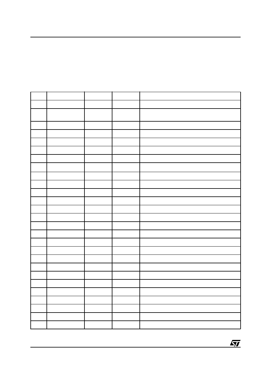
2.0 PACKAGING AND PIN INFORMATION
2.1 STLC1511 Pin Allocation
The pinout for the STLC1511 is depicted in Figure 1.
TQFP64
ORDERING NUMBER: STLC1511
PRODUCT PREVIEW
NorthenLiteTM G.lite BiCMOS
Analog Front-End Circuit
Figure 1. STLC1511 pinout
1
2
3
5
6
4
7
8
9
10
27
11
28 29 30 31 32
59 58 57 56
54
55
53 52 51 50 49
43
42
41
39
38
40
48
47
46
44
45
VSSDIGE1
RXSOUT[1]
RXSOUT[0]
CK35M
VDDDIG1
DIGREF
DIGCLK
DTX
VDDDIG2
VSSDIG2
VDDDIGE1
RXDCINP
RXDCINN
RXDCON
RXDCOP
RXINP
RXINN
RXOPIINN
RXOPINP
VCCRXPGA
VEERXPGA
QVEERX
QVEEDAC
TXDADC1
VEEDAC
VCCDAC
VDDESD2
VSSESD2
VEETXPGA
VCCTXPGA
TXON
TXOP
QVEETX
VCCPLL
VEEPLL
FREQ
OSCNB
OSCPB
OSCNE
QVEEBIAS
VEEBIAS
VCCBIAS
V3P75V
IREF50m
TQFP64
22 23 24 25 26
60
RESETN
61
TXSIN[0]
62
TXSIN[1]
63
FRMCLK
64
VSSDIG1
ADCDC3
ADCDC2
ADCDC1
VSSESD1
VDDESD1
17 18 19 20 21
37
36
34
33
35
OSCPE
VCAP
VSSPLL
QVEEPLL
VDDPLL
12
13
14
15
16
QVEEADC
VCCADC
VEEADC
ENB
DRX
STLC1511
2/31
2.2 Pin Description
Table 1. details the pinout assignment for the
STLC1511. The following list gives the different pin
types for the STLC1511.
s
VDD/VCC - 5V power supply
s
VEE/VSS - Ground supply
s
DO/DI - Digital Output/ Digital Input
s
AO/AI/AIO - Analog Output/ Analog Input/
Analog Input-Output
Table 1. Pin Assignement
Pin #
Pin Name
Pin Type
Pad Type
Description
1
VDDDIG1
VDD
VDDCO
5V supply (digital) for ADC and DAC
2
CK35M
DI
TLCHT
35.328MHz serial interface clock input (also used in
Test Mode to test PFD. See Table on page 21)
3
DIGREF
DO
BT4CR
35.328/17.644MHz reference for Digital ASIC PLL
4
RXSOUT[0]
DO
BT4CR
Rx serial data (lsb) output
5
RXSOUT[1]
DO
BT4CR
Rx serial data (msb) output
6
VSSDIGE1
VSS
VSSE
Ground for digital output drivers
7
VSSDIG2
VSS
VSSCO
Ground supply for digital interface, serial interface
8
VDDDIGE1
VDD
VDDE
5 V supply for digital output drivers
1
9
VDDDIG2
VDD
VDDCO
5 V supply for digital interface, serial interface
10
DTX
DO
BT4CR
Data Output for digital interface
11
DIGCLK
DI
TLCHT
35.328MHz clock input for digital interface
12
ENB
DI
TLCHT
Enable input for digital interface
13
DRX
DI
TLCHT
Data Input for digital interface
14
VEEADC
VEE
VSSCO
Ground for ADC
15
VCCADC
VCC
VDDCO
5 V supply for ADC
16
QVEEADC
VEE
VSSCO
Quiet ground for ADC circuitry
17
ADCDC3
AIO
ANA
ADC reference decoupling (3.75 V) 0.1uF
18
ADCDC2
AIO
ANA
ADC reference decoupling (2.5 V) 0.1uF
19
ADCDC1
AIO
ANA
ADC reference decoupling (1.25 V) 0.1uF
20
VSSESD1
VSS
VSSA
Ground for ESD ring
21
VDDESD1
VDD
VDDA
5 V supply for ESD ring
22
RXDCINP
AI
ANA
RxPGA positive input from DC blocking capacitor
23
RXDCINN
AI
ANA
RxPGA negative input from DC blocking capacitor
24
RXDCON
AO
ANA
RxPGA negative output to DC blocking capacitor
25
RXDCOP
AO
ANA
RxPGA positive output to DC blocking capacitor
26
RXINN
AI
ANA
Rx negative input (AC coupled)
27
RXINP
AI
ANA
Rx positive input (AC coupled)
3/31
STLC1511
28
RXOPINN
AI
ANA
Rx opamp negative input (must be DC coupled)
29
RXOPINP
AI
ANA
Rx opamp positive input (must be DC coupled)
30
VCCRXPGA
VCC
VDDCO
5V supply for RxPGA
31
VEERXPGA
VEE
VSSCO
Ground for RxPGA
32
QVEERX
VEE
VSSCO
Quiet ground for Rx circuitry
33
QVEEPLL
VEE
VSSCO
Quiet ground for PLL circuitry
34
VSSPLL
VSS
VSSCO
Ground for Oscillator
2
35
VDDPLL
VDD
VDDCO
5 V supply for Oscillator
2
36
VCAP
AO
ANA
Charge pump output to varactor
37
OSCPE
AIO
ANA
Oscillator I/O (emitter)
38
OSCPB
AIO
ANA
Oscillator I/O (base)
39
OSCNB
AIO
ANA
Oscillator I/O (base)
40
OSCNE
AIO
ANA
Oscillator I/O (emitter)
41
FREF
AI
ANA
2.56 MHz PLL input reference/ 35.328 MHz clock
input
42
VEEPLL
VEE
VSSCO
Ground for oscillator
2
43
VCCPLL
VCC
VDDCO
5 V supply for oscillator
2
44
V3P75V
AIO
ANA
3.75V output from Bandgap to 0.22mF capacitor
45
IREF50m
AIO
ANA
External resistor for bias current R=2.5V/
50mA=50kohm
46
VCCBIAS
VCC
VDDCO
5V supply for biasing
47
VEEBIAS
VEE
VSSCO
Ground for biasing
48
QVEEBIAS
VEE
VSSCO
Quiet ground for bias circuitry
49
QVEETX
VEE
VSSCO
Quiet ground for Tx circuitry
50
TXOP
AO
ANA
Tx positive output
51
TXON
AO
ANA
Tx negative output
52
VCCTXPGA
VCC
VDDCO
5V supply for TxPGA
53
VEETXPGA
VEE
VSSCO
Ground for TxPGA
54
VDDESD2
VDD
VDDA
5V supply for ESD ring
55
VSSESD2
VSS
VSSA
Ground for ESD ring
56
VCCDAC
VCC
VDDCO
5V supply for DAC
57
VEEDAC
VEE
VSSCO
Ground for DAC
58
TXDADC1
AIO
ANA
DAC reference (2.5V) 0.1uF
Table 1. Pin Assignement
Pin #
Pin Name
Pin Type
Pad Type
Description
STLC1511
4/31
59
QVEEDAC
VEE
VSSCO
Quiet ground for DAC circuitry
60
RESETN
DI
TLCHT
ResetN for the AFE
61
TXSIN[0]
DI
TLCHT
Tx serial data (lsb) input
62
TXSIN[1]
DI
TLCHT
Tx serial data (msb) input
63
FRMCLK
DO
BT4CR
Tx 4.416MHz frame clock reference output
64
VSSDIG1
VSS
VSSCO
Ground (digital) for ADC and DAC
<1>HCMOS5 guidelines are for 1 pair of power/ground for 4 output drivers (4mA)
<2>Pins 35 and 43 are both connected to the analog VCC supplying the on chip oscillator. Similarly, Pins 34 and 42 are connected
to analog VSS for the oscillator. Supply line inductance is reduced using two pads for VCC (and VSS) in this manner. At the board
level, Pins 35 and 43 should be connected to analog VCC, and pins 34 and 42 should be connected to analog VSS.
Table 1. Pin Assignement
Pin #
Pin Name
Pin Type
Pad Type
Description
3.0 FUNCTIONAL DESCRIPTION
3.1 General Functional Description
The STLC1511 consists of the following functional
blocks:
s
Transmit Signal Path
s
Receive Signal Path
s
Phase Lock Loop and Amplifier for an external
oscillator.
s
Bias Voltage and Current Generation
s
Digital Interface
s
Serial Interface
The transmit path contains the 14-bit digital to analog
converter (DAC) necessary to generate the transmit
signal from a 14-bit digital input word. This transmit
signal is then scaled by the on chip programmable
gain amplifier (TxPGA) from 0 to -32dB in 2dB steps.
The scaled output signal is then driven off chip to the
external filters and power amplifier (PA) which drives
the DMT signal to the subscriber loop. The transmit
path is fully differential but may be used single ended
if both outputs from the TxPGA are terminated cor-
rectly.
The receive path contains an optional unity gain buff-
er followed by a two stage programmable gain ampli-
fier (RxPGA), a 1st order low pass anti-aliasing filter,
and a 12-bit analog to digital converter (ADC). The
RxPGA consists of two stages and the gain is digitally
programmable from 0 to 40dB in 0.5dB steps. The re-
ceive path is fully differential but may be used single
ended provided the other input to the RxPGA is
grounded.
The STLC1511 contains the circuits required to con-
struct a PLL that generates either a 17.644MHz/
35.328 MHz clock from a 2.56 MHz reference clock
when supplied with an external LC or crystal oscilla-
tor and tuning circuit. This clock is supplied to the
both the transmit and receive converters, and the se-
rial interface used to transfer the Rx/Tx data between
the STLC1511 and digital chip. The STLC1511 also
has the ability to be driven directly by an external
35.328MHz clock supplied to the FREF pin.
The bias circuitry contains a bandgap voltage refer-
ence from which the converter references and analog
ground voltage is generated. This block also gener-
ates an accurate current using an external resistor
from which all of the STLC1511 circuits are biased. In
addition, the bias circuitry also generates a 2.5V ref-
erence for the external Vco/Vcxo components and
can be used for other external circuits if necessary.
There is a 4 pin serial digital interface (DTX, DRX,
DIGCLK, ENB) that loads a one of four 8-bit control
register that controls all the programmable features
on the STLC1511. Refer to "Digital Interface And
Memory Map" on page 20 for more information on
the programmability of the AFE.
To facilitate data transfer between the STLC1511
and the digital ASIC (STLC1510), a 2-bit wide serial
interface for the transmit path and a 2-bit wide serial
interface for the receive path is incorporated into the
AFE. This interface consists of two transmit pins (TX-
SIN[0:1]), two receive pins (RXSOUT[1:0]), and the
necessary control signals (FRMCLK, CK35M) to
transmit the required data. For more information See
"Serial Interface" on page 18.
5/31
STLC1511
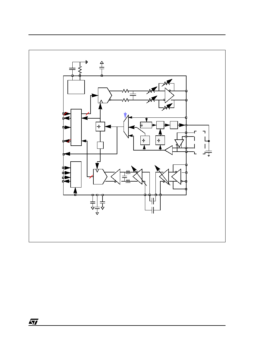
Figure 2. The block diagram of the STLC1511
3.2 Receive Path Specifications
Note: The first stage of the RxPGA provides a coarse gain of 0/20dB with a differential input or 6/26dB with a
single ended input. The second stage implements a programmable gain from 0dB to 20dB in 0.5dB steps.
12
14
D
i
g
ita
l
I
/
F
Ser
i
a
l
I
/
F
B a nd ga p/
Bias Gen
14 -bit
12 -b it
A D C
D A C
4.416M
4.416M
35.328M /
5
8/4
69
2.56M /35.328M
2.56M
35.328M
(Externa l Clock M ode)
(O scillator M ode)
D I G C L K
E N B
D R X
R X IN N
R X I N P
RXD
CO
P
R
XDC
O
N
R
XDC
I
P
R
XDC
I
N
T X SIN [1:0]
F R M C L K
R X S O U T [1:0]
C K 3 5 M
V3
P
5
V
I
R
E
F
50U
0.22
uF
50
k
T X O P
T X O N
F R E F
V C A P
2
2
R
E
S
ETN
E x
te
rn
al
R
es
on
at
or
G
O S C N E
O S C P E
O S C P B
O S C N B
di
g
I/
F
D T X
90
∞
D IG R E F
17.622M
R X O P IN P
R X O P I N N
+
-
2 /3 /4 /8
PFD
C P
+
-
G =1
fp=2M H z
fp= 2M H z
AD
CDC
1
A
DCD
C2
AD
CDC
3
T
X
D
ADC
1
0.
1u
F
0.
1u
F
0.1
uF
0.1u
F
0.1
uF
0.1u
F
+
-
+
-
+
-
Shaded blocks are only usabe when the PLL is active. Crystal based external resonator for the CPE Mode, LC
based resonator for the CO Oscillator Mode. 35.328 MHz external reference in CO External Clock Mode.