1/26
STLC1512
November 2000
This is preliminary information on a new product now in development. Details are subject to change without notice.
s
Low power architecture -- Class AB, current
drive, output stage through a centre tapped
transformer to facilitate power supply switching
between 5.0V and a lower voltage. (3.3V in the
reference design) This gives a reduction in
power consumption.
s
480mW power consumption with a typical G.lite
signal.
s
600mA current driving capability
s
Positive +5.0V and one lower supply. (3.3V in
the reference design)
s
Switching power supplies to save power
s
Thermal overload shutdown
s
Four programmable receive gains
s
Opamp for a low pass filter in the receive path
s
Undedicated opamp with separate power down
control (used as a transmit path filter in the
reference design)
s
Separate power down control for Tx and Rx
path
s
48-pin TQFP (7x7x1.4mm) package
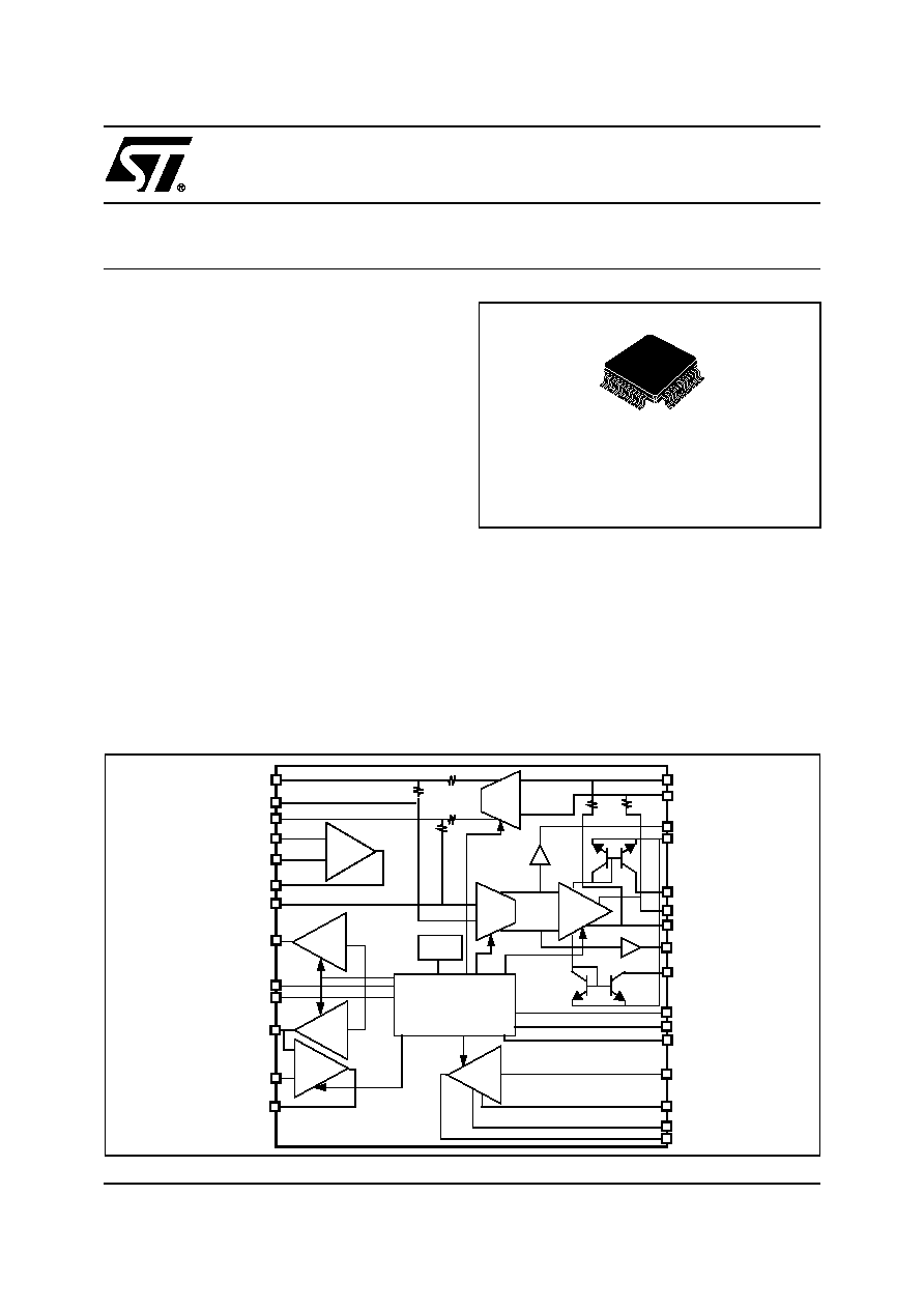
1.0 GENERAL DESCRIPTION
The STLC1512 G.lite line driver chip contains the line
driver as well as part of the receive path required in a
central office G.lite modem. It provides an interface
between the AFE chip (STLC1511) and the tele-
phone line. The line driver chip has been designed
with low power consumption, high signal to noise
plus distortion ratio and high current driving capabili-
ty.
TQFP48 (7x7x1.40)
ORDERING NUMBER: STLC1512
PRODUCT PREVIEW
NorthenLiteTM G.lite Loop Driver
Figure 1. Block Diagram
TXANG
RBIAS
RXPD
LPFOUT
LPFIN
REF2P5
DCFBON
DCFBOP
FPN
FPP
PAIP
PAIN
PWRVEEx
PAOPx
BUFFP
BUFFN
PAONx
PGA
RX REF
Buffer
LPF AMP
BIAS
Thermal
Shutdown
Preamp
Power
Stage
DC
Feedback
Amp
OPAMP
TX REF
Buffer
AMPPD
TXPD
PGAIN
PGA1
PGA0
RXANG
DCFBIN
DCFBIP
AMPIP
AMPIN
AMPOUT
PGAOUT
STLC1512
2/26
1.0 GENERAL DESCRIPTION
The line driver transmit path contains a preamplifier
followed by a power output stage. The power stage
has current outputs that directly drive the primary
side of a center tapped transformer.
The receive path contains a programmable gain am-
plifier followed by an opamp which is used with off
chip passive components in an active low pass filter.
The Programmable Grain Amplifier (PGA) has four
steps optimized for the recommended G.lite CO line
interface.
There is also an undedicated opamp which can be
used for active filtering in either the transmit or re-
ceive paths
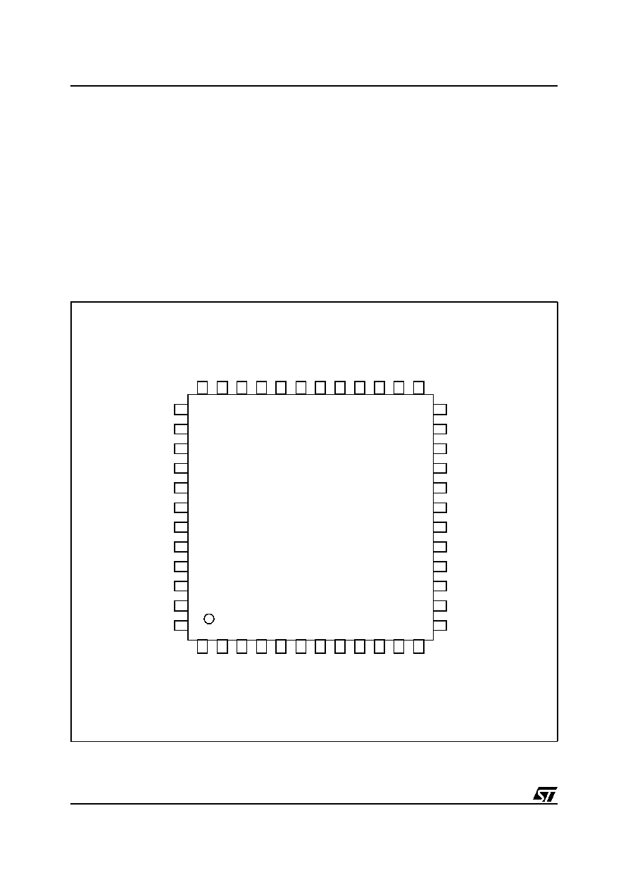
2.0 PACKAGING AND PIN INFORMATION
2.1 Package Technology
STLC1512 will be packaged in a TQFP 48 package,
according to JEDEC Specification reference MS-
026-BBC.
2.2 STLC1512 Pin Allocation
The pin out for the STLC1512 is depicted in the fol-
lowing Figure 2.
Figure 2. STLC1512 pinout
NC
48
1
TQFP48 (7x7x1.4mm)
TXANG
RBIAS
PGA
O
U
T
PG
A
I
N
R
XAN
G
R
XVC
C
1
R
XVC
C
2
R
XVEE
1
TX
P
D
QVEER
X
PG
A1
PGA0
R
XVEE
2
AM
PPD
RXPD
LPFOUT
LPFIN
NC
REF2P5
DCFBON
DCFBOP
FPN
FPP
PAIP
PAIN
AM
PI
P
AM
PI
N
AM
PO
U
T
T
XVC
C
3
T
XVC
C
2
T
XVC
C
1
T
XVE
E1
T
XVE
E2
T
XVE
E3
QVE
E
T
X
DC
FB
I
P
DC
FB
I
N
PWRVEE1
PWRVEE2
PAOP1
PAOP2
BUFFP
BUFFN
PAON1
PAON2
PWRVEE3
PWRVEE4
3/26
STLC1512
2.3 Pin Description
The pin description for the STLC1512 is given in the following Table 1.
Table 1. Pin Description
Pin #
Pin Name
Pin Type
Pin Description
1
1
PGAOUT
AO
Rx PGA output (programmable gain amplifier)
2
PGAIN
AI
Rx PGA input
3
RXANG
AO
2.5V Rx buffered reference
4
RXVCC1
VCC
+5.0V supply for Rx path circuitry
5
RXVCC2
VCC
+5.0V supply for Rx path circuitry
6
QVEERX
VEE
Quiet ground for the Rx circuitry
7
RXVEE1
VEE
Ground for Rx path circuitry
8
RXVEE2
VEE
Ground for Rx path circuitry
9
PGA0
DI
PGA gain setting control bit 0
10
PGA1
DI
PGA gain setting control bit 1
11
TXPD
DI
Tx path power down control (Active low)
12
AMPPD
2
DI
Undedicated opamp power down control (Active low)
13
RXPD
DI
Rx path power down control (Active low)
14
PWRVEE4
VEE
Power stage ground.
15
PWRVEE3
VEE
Power stage ground.
16
PAON2
AO
Tx Power Amplifier Negative output
17
PAON1
AO
Tx Power Amplifier Negative output
18
BUFFN
AO
Current generator buffer negative output
19
BUFFP
AO
Current generator buffer positive output
20
PAOP2
AO
Tx Power Amplifier Positive output
21
PAOP1
AO
Tx Power Amplifier Positive output
22
PWRVEE2
VEE
Power stage ground.
23
PWRVEE1
VEE
Power stage ground.
24
NC
Not connected
25
DCFBIN
AI
Power amp DC feedback amplifier negative input
26
DCFBIP
AI
Power amp DC feedback amplifier positive input
27
QVEETX
VEE
Quiet ground for Tx circuitry
28
TXVEE3
VEE
Ground for Tx path circuitry
29
TXVEE2
VEE
Ground for Tx path circuitry
30
TXVEE1
VEE
Ground for Tx path circuitry
31
TXVCC1
VCC
+5.0V supply for power amp output stage
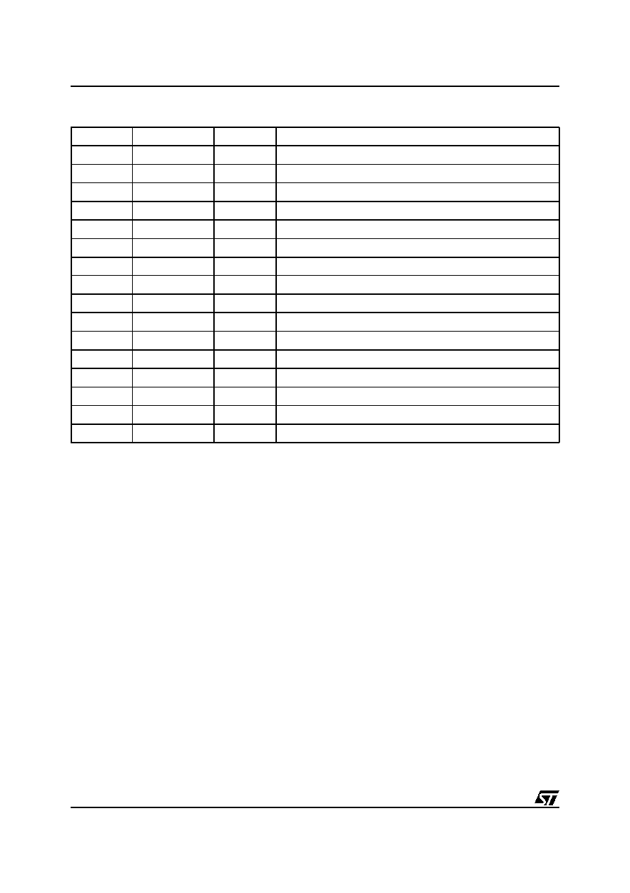
STLC1512
4/26
32
TXVCC2
VCC
+5.0V supply for power amp output stage
33
TXVCC3
VCC
+5.0V supply for Tx path circuitry and bias blocks
34
AMPOUT
AO
Undedicated opamp output
35
AMPIN
AI
Undedicated opamp negative input
36
AMPIP
AI
Undedicated opamp positive input
37
DCFBON
AO
Power amp DC feedback amplifier negative output
38
DCFBOP
AO
Power amp DC feedback amplifier positive output
39
TXANG
AO
2.5V Tx buffered reference
40
FPP
AO
Fast path positive output
41
FPN
AO
Fast path negative output
42
PAIP
AI
Tx Power amplifier positive input
43
PAIN
AI
Tx Power amplifier negative input
44
RBIAS
AO
Reference resistor generating bias current
45
REF2P5
AI
Externally supplied 2.5V reference
46
NC
Not connected
47
LPFOUT
AO
LPF (low pass filter) Op Amp output
48
LPFIN
AI
LPF (low pass filter) Op Amp negative input
<1>The values of the components that are connected to the pins are shown in Figure 11.
<2>If the undedicated opamp is used in the transmit path, AMPPD can be connected to TXPD on the board. If the undedicated opamp
is used in the receive path, AMPPD can be connected to RXPD on the board. This opamp is powered off of TXVCC3.
Table 1. Pin Description
3.0 FUNCTIONAL DESCRIPTION
The STLC1512 consists of the following functional
blocks:
s
Transmit Signal Path
s
Receive Signal Path
s
Thermal Protection
The transmit signal that comes from the AFE is fil-
tered before it reaches the line driver. STLC1512
contains an opamp that can be utilized as part of this
filter. The AMPPD pin allows this op amp to be pow-
ered down independently. The line driver consists of
a preamp followed by a current drive power stage.
The preamplifier provides large open loop gain while
the power stage provides open collector current drive
to allow for single supply switching. The center tap of
the primary side of the transformer is connected to a
supply that can be switched between 5.0V and a low-
er supply to realize power savings on a DMT signal.
The reference design sets this supply at 3.3V. The
line driver can be powered down by a low at the
TXPD pin.
The receive path consists of a Programmable Gain
Amplifier (PGA) and an active low pass filter. The
PGA is programmable in four steps. The active low
pass filter is composed of an on chip op amp and ex-
ternal passive components. The receive signal pass-
es through the PGA, is low pass filtered and then
driven off chip to the AFE chip. Both the PGA and the
opamp can be powered down by RXPD signal.
A thermal protection circuit has also been implement-
ed on the chip to prevent the chip from overheating
under fault conditions.
4.0 SPECIFICATIONS
4.1 Chip Specifications
The cross-talk specifications are based on the as-
sumption that cross-talk should not degrade the
SNDR of the receive signal. If there is receive cross-
talk into the transmit path, this signal will come back
through the hybrid balance and cause noise in the re-
ceive path. If the signal is undistorted it will cause a
small gain and phase error which will not affect per-
formance. If it is distorted it will cause an increased
5/26
STLC1512
noise floor which will degrade the SNDR of the re-
ceive signal.
The same is true of the transmit signal. If the signal is
undistorted it will show up out of band in the receive
path and will not degrade SNDR. However, if the
transmit signal is distorted by the cross-talk mecha-
nism it will show up in the receive band and could re-
duce the SNDR.
The cross-talk numbers are specified from output to
output under maximum gain conditions.
4.2 Power Amplifier Performance
Specifications
The power amplifier must be specified with all of the
external components in the application diagram.
Without these components the amplifier will not func-
tion correctly. Specifications that are measured at the
chip are specified as such in the comments.
Table 3 contains the conditions over which the spec-
ifications in Table 4 apply. The limits on the specifica-
tions in Table are valid over all of the ranges
specified in Table 3. The nominal values of the spec-
ification occur at the nominal value of all of the condi-
tions in Table 3 unless otherwise specified.
...
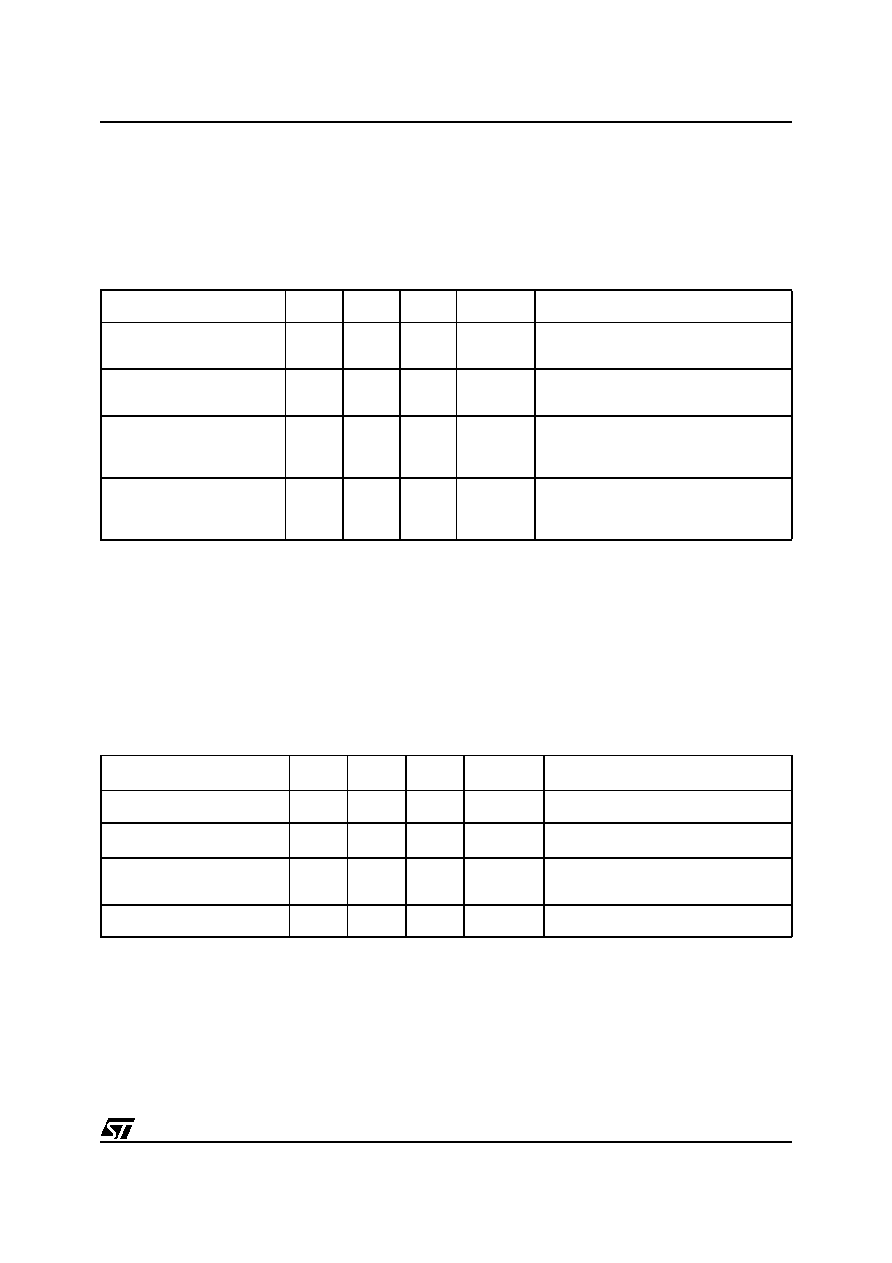
Table 2. Chip Performance Specifications
Description
min
nom
max
Units
Comments
Rx Cross-Talk into Tx
Undistorted
-55
dB
Measured from the active low pass filter
output in the receive path to tip and ring.
Rx Cross-Talk into Tx
Distorted
-73
dB
Measured from the active low pass filter
output in the receive path to tip and ring.
Tx Cross-talk into Rx
Undistorted
-50
dB
Measured from tip and ring to the active
low pass filter output with the maximum
gain setting in place.
Tx Cross-talk into Rx
Distorted
-86
dB
Measured from tip and ring to the active
low pass filter output with the maximum
gain setting in place.
Table 3. Power Amplifier Performance Limits
Description
min
nom
max
Units
Comments
1
,
2
Gain
19.9
20.1
20.3
dB
Ambient Temperature
-40
27
85
o
C
Line Impedance
80
100
160
W
A nominal chip will have no problem
driving 200
or 50
.
Supply voltage for TXVCC
4.75
5.0
5.25
V
<1>Nominal specifications are for nominal bias and process
<2>Maximum and minimum specifications are for worst case process and bias conditions