 | –≠–ª–µ–∫—Ç—Ä–æ–Ω–Ω—ã–π –∫–æ–º–ø–æ–Ω–µ–Ω—Ç: STLC2410 | –°–∫–∞—á–∞—Ç—å:  PDF PDF  ZIP ZIP |
1/20
STLC2410B
June 2003
This is preliminary information, details are subject to change without notice.
1
FEATURES
s
Bluetooth
Æ
V1.1 specification compliant
s
Point-to-point, point-to-multi-point (up to 7
slaves) and scatternet capability
s
Asynchronous Connection-Less (ACL) link
support giving data rates up to 721kbps
s
Synchronous Connection-Oriented (SCO) link
s
Standard BlueRF bus interface
s
ARM7TDMI CPU
≠ 32-bit Core
≠ Run from 13MHz external clock
≠ Support of 32 kHz crystal for low power mode
s
Memory organization
≠ 64KByte on-chip RAM
≠ 4KByte on-chip boot ROM
≠ Programmable external memory interface (EMI)
≠ 8-bit or 16-bit external data bus
≠ Up to 3 programmable chip-select signals
≠ Hold-acknowledge bus arbitration support
s
HW support for all packet types
≠ ACL: DM1, 3, 5 and DH1, 3, 5
≠ SCO: HV1, 2, 3 and DV1
s
Communication interfaces
≠ Serial Synchronous Interface
≠ Two enhanced 16550 UART's with 128 byte
fifo depth
≠ 12Mbps USB interface
≠ Fast master I2C bus interface
≠ Multi slot PCM interface
≠ 16 programmable GPIO
≠ 2 external interrupts and various interrupt
possibilities through other interfaces
s
Ciphering support for up to 128-bit key
s
Receiver Signal Strenght Indication (RSSI)
support for power-controlled links
s
Separate control for external power amplifier
(PA) for power class1 support.
s
Software support
≠ Low level (up to HCI) stack or embedded
stack with profiles
≠ Support of UART and USB HCI transport layers
s
Idle and power down modes
≠ Ultra low power in idle mode
≠ Low standby current
1.1 Applications Features
Typical applications in which the STLC2410B can
be used are:
s
Portable computers, PDA
s
Modems
s
Handheld data transfer devices
s
Cameras
s
Computer peripherals
s
Other type of devices that require the wireless
communication provided by Bluetooth
Æ
s
Cable replacement
2
DESCRIPTION
The STLC2410B offers a compact and complete
solution for short-range wireless connectivity. It in-
corporates all the lower layer functions of the Blue-
tooth
Æ
protocol.
The microcontroller allows the support of all data
packets of Bluetooth
Æ
in addition to voice. The em-
bedded controller can be used to run the Blue-
tooth
Æ
protocol and application layers if required.
The software is located in an external memory ac-
cessed through the external memory interface.
TFBGA132 (8x8x1.2mm)
ORDERING NUMBER: STLC2410B
Temperature range: -40 to +85 ∞C
PRELIMINARY DATA - REV. 1.1
BLUETOOTH
Æ
BASEBAND
STLC2410B
2/20
3
QUICK REFERENCE DATA
3.1 Absolute Maximum Ratings
Operation of the device beyond these conditions is not guaranteed.
Sustained exposure to these limits will adversely affect device reliability
Table 1. Absolute Maximum Ratings
3.2 Operating Ranges
Operating ranges define the limits for functional operation and parametric characteristics of the device.
Functionality outside these limits is not implied.
Table 2. Operating Ranges
3.3 I/O specifications
Depending on the interface, the I/O voltage is typical 1.8V (interface to the flash memory) or typical 3.3V
(all the other interfaces). These I/Os comply to the EIA/JEDEC standard JESD8-B.
3.3.1 Specifications for 3.3V I/Os
Table 3. LVTTL DC Input Specification (3V<V
DDIO
<3.6V)
Table 4. LVTTL DC Output Specification (3V<V
DDIO
<3.6V)
Note 1 : X is the source/sink current under worst case conditions according to the drive capability. (See table 8, pad information for value of X).
Symbol
Conditions
Min
Max
Unit
V
DD
Supply voltage core
V
SS
- 0.5
2.5
V
V
DDIO
Supply voltage I/O
4
V
V
IN
input voltage on any digital pin
V
SS
- 0.5
V
DDIO
+ 0.3
V
T
amb
Operating ambient temperature
-40
+85
∞
C
T
stg
Storage temperature
-65
+150
∞
C
T
lead
Lead temperature < 10s
+240
∞
C
Symbol
Conditions
Min
Typ
Max
Unit
V
DD
Supply voltage digital core and emi pads
1.55
1.8
1.95
V
V
DDIO
Supply voltage digital IO
2.7
3.3
3.6
V
Symbol
Parameter
Conditions
Min
Typ
Max
Unit
V
il
Low level input voltage
0.8
V
V
ih
High level input voltage
2
V
V
hyst
Schmitt trigger hysteresis
0.4
V
Symbol
Parameter
Conditions
Min
Typ
Max
Unit
Note
V
ol
Low level output voltage
I
ol
= X mA
0.15
V
1
V
oh
High level output voltage I
oh
=-X mA
V
DDIO
-0.15
V
1

3/20
STLC2410B
3.3.2 Specifications for 1.8V I/Os
Table 5. DC Input Specification (1.55V<V
DD
<1.95V)
Table 6. DC Output Specification (1.55V<V
DD
<1.95V)
Note 1 : X is the source/sink current under worst case conditions according to the drive capability. (See table 8, pad information for value of X).
3.4 Current Consumption
Table 7. Typical power consumption of the STLC2410B and External Flash using UART (VDD =
VDD Flash = PLLVDD = 1.8V, VDDIO = 3.3V)
Symbol
Parameter
Conditions
Min
Typ
Max
Unit
V
il
Low level input voltage
0.35*V
DD
V
V
ih
High level input voltage
0.65*V
DD
V
V
hys
t
Schmitt trigger hysteresis
0.2
0.3
0.5
V
Symbol
Parameter
Conditions
Min
Typ
Max
Unit
Note
V
ol
Low level output voltage
I
ol
= X mA
0.15
V
1
V
oh
High level output voltage
I
oh
=-X mA
V
DD
-0.15
V
1
STLC2410B State
Core
IO
Unit
Slave
Master
Standby (no low power mode)
5.10
5.10
0.13
mA
Standby (low power mode enabled)
0.94
0.94
0.13
mA
ACL connection (no transmission)
7.60
6.99
0.13
mA
ACL connection (data transmission)
7.90
7.20
0.13
mA
SCO connection (no codec connected)
8.70
7.90
0.14
mA
Inquiry and Page scan (low power mode enabled)
127
n.a.
5
µ
A
Low Power mode (32 kHz crystal)
20
20
0
µA
STLC2410B
4/20
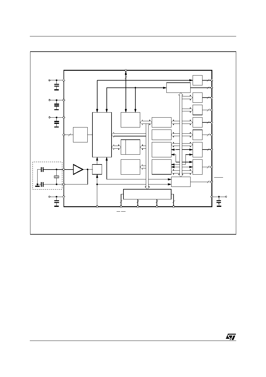
Figure 1. Block Diagram and Electrical Schematic
RADIO
I/F
BLUETOOTH
CORE
Æ
ARM7
TDMI
APB
BRIDGE
INTERRUPT
CONTROLLER
TIMER
START
DETECT
UART
FIFO
SYSTEM
CONTROL
EMI
UART
UART
100nF
100nF
22pF
Y2
32KHz
(*) If a low-power clock is available, it can be connected to the LPOCLKP pin in stead of using a crystal
22pF
GPIO
BOOT
ROM
D
M
A
RAM
LPO
13
4
RF BUS
PCM
EXT._INT1/2
USB
I
2
C
SPI
GPIO(O..15)
UART2
UART1
V
DD
RESET
SYS_CLK_REQ
LPOCLKP
LPOCLKN
VDDPLL
SPI
I
2
C
USB
PCM
2
2
4
4
5
JTAG
XIN
BOOT WAIT
RD/WR
CSN(0..2)
ADDR(0..19) DATA(0..15)
3
20
16
16
8
2
2
2
D02TL550
V
DD
100nF
V
DDIO
100nF
V
DDIO
100nF
V
DD
(*)
5/20
STLC2410B
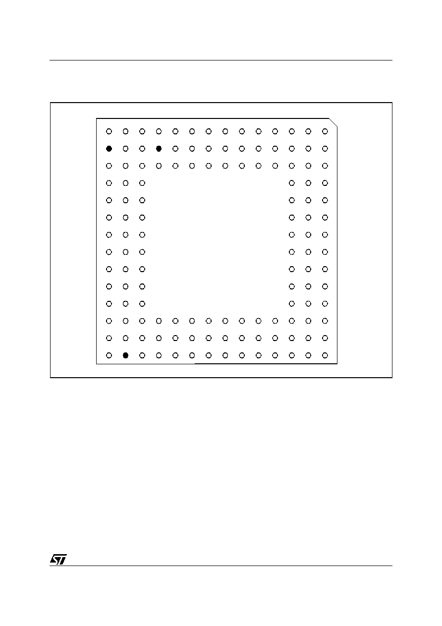
4
PINOUT
Figure 2. Pinout (Bottom view)
4.1 Pin Description and Assignment
Table4 : STLC2410B pinlist shows the pinout of STLC2410B; there are 107 digital functional pins and 22
supply pins. The column "PU/PD" shows the pads implementing an internal weak pull-up/down, to fix value
if the pin is left open. This can not replace an external pull-up/down.
The pads are grouped according to two different power supply values, as shown in column "VDD":
≠ V1 for 3.3 V typical 2.7 - 3.6 V range
≠ V2 for 1.8 V typical 1.55 - 1.95 V range
Finally the column "DIR" describes the pin directions:
≠ I for inputs
≠ O for outputs
≠ I/O for input/outputs
≠ O/t for tristate outputs
D02TL551
A
B
C
D
E
F
G
H
J
K
L
M
N
P
14
13
12
11
10
9
8
7
6
5
4
3
2
1
gpio9 gpio11 gpio14 vddio
brxd bmosi bdclk bpaen brxen ant_sw
tdi
ntrst
test
xin
n.c. gpio10 gpio13 n.c.
brclk bnden btxd
vdd
btxen vddio
tdo
tck
nreset
gpio8 vddpll gpio12
vsspll gpio6 gpio7
gpio3 gpio4 gpio5
gpio0 gpio1 gpio2
boot
vddio vssio
pcm_
sync
i2c_clk int1
int2
pcm_
clk
lpo_
clk_p
lpo_
clk_n
data
14
uart2_
txd
uart2_
i1
uart2_
i2
uart2_
o1
uart2_
io2
uart2_
o2
uart2_
io1
data
15
wait
data
13
data
12
data
11
data
10
data
9
vss
vss
vss
vdd
vdd
vdd
vssio
spi_frm
vddio
usb_
dn
uart2_
rxd
usb_
dp
pcm_a pcm_b
gpio15 vssio bmiso bsen
vss bpktctl vssio
tms
data8 data7 data6 data0 addr17 vss
addr13 addr10 addr5 addr2
vdd
csn1
uart1_
rxd
uart1_
txd
i2c_
dat
spi_
txd
spi_
clk
data5 data4 data2 addr19 addr16 vdd addr12 addr9 addr6 addr3
vss
csn2
wrn
spi_
rxd
data3
n.c.
data1 addr18 addr15 addr14 addr11 addr8 addr7 addr4 addr1 addr0 csn0
rdn
sys_
clk_req