1/27
STLC2416
June 2004
This is preliminary information on a new product now in development or undergoing evaluation. Details are subject to change without notice.
1
FEATURES
Pin to pin compatible with the previous version
STLC2415
Ericsson Technology Licensing Baseband Core
(EBC)
BluetoothTM specification compliance: V1.1 and V1.2
SW compatible with STLC2411-M28R400CT
combination
2 layer class 4 PCB compatible
Point-to-point, point-to-multi-point (up to 7
slaves) and scatternet capability
Asynchronous Connection Oriented (ACL)
logical transport link
Synchronous Connection Oriented (SCO) links:
2 simultaneous SCO channels
Supports Pitch-Period Error Concealment (PPEC)
� Improves speech quality in the vicinity of in-
terference
� Improves coexistence with WLAN
� Works at receiver, no Bluetooth implication
Adaptive Frequency Hopping (AFH): hopping
kernel, channel assessment as Master and as
Slave
Faster Connection: Interlaced scan for Page
and Inquiry scan, first FHS without random
backoff, RSSI used to limit range
Extended SCO (eSCO) links
Standard BlueRF bus interface
QoS Flush
Clock support
� System clock input:
any integer value from 12 ... 33 MHz
� LPO clock input at 3.2 and 32 kHz or via the
embedded 32 kHz crystal oscillator cell
ARM7TDMI 32-bit CPU
Memory organization
� Integrated 4Mbit flash
� 64KByte on-chip RAM
� 4KByte on-chip boot ROM
Low power architecture with 2 different low power
levels:
� Sleep Mode
� Deep Sleep Mode
HW support for packet types
� ACL: DM1, 3, 5 and DH1, 3, 5
� SCO: HV1, 3 and DV
� eSCO: EV3, 5
Communication interfaces
� Synchronous Serial Interface, supporting up
to 32 bit data and different industry standards
� Two enhanced 16550 UARTs with 128 byte
FIFO depth
� 12Mbps USB interface
� Fast master I2C bus interface
� Multi slot PCM interface
� 16 programmable GPIOs
� 2 external interrupts and various interrupt
possibilities through other interfaces
Efficient support for WLAN coexistence in
collocated scenario
Ciphering support for up to 128-bit key
Receiver Signal Strength Indication (RSSI)
support for power-controlled links
Separate control for external power amplifier
(PA) for class1 power support.
Software support
� Low level (up to HCI) stack or embedded
stack with profiles
� Support of UART and USB HCI transport layers.
1.1 Applications Features
Typical applications in which the STLC2416 can
be used are:
Cable replacement
Portable computers, PDA
Modems
Handheld data transfer devices
Cameras
Computer peripherals
Other type of devices that require the wireless
communication provided by BluetoothTM
PRELIMINARY DATA
BLUETOOTHTM BASEBAND WITH INTEGRATED FLASH
Figure 1. Package
Table 1. Order Codes
Part Number
Package
Temp. Range
STLC2416
LFBGA120
-40 to +85 �C
LFBGA120 (10x10x1.4mm)
REV. 1
STLC2416
2/27
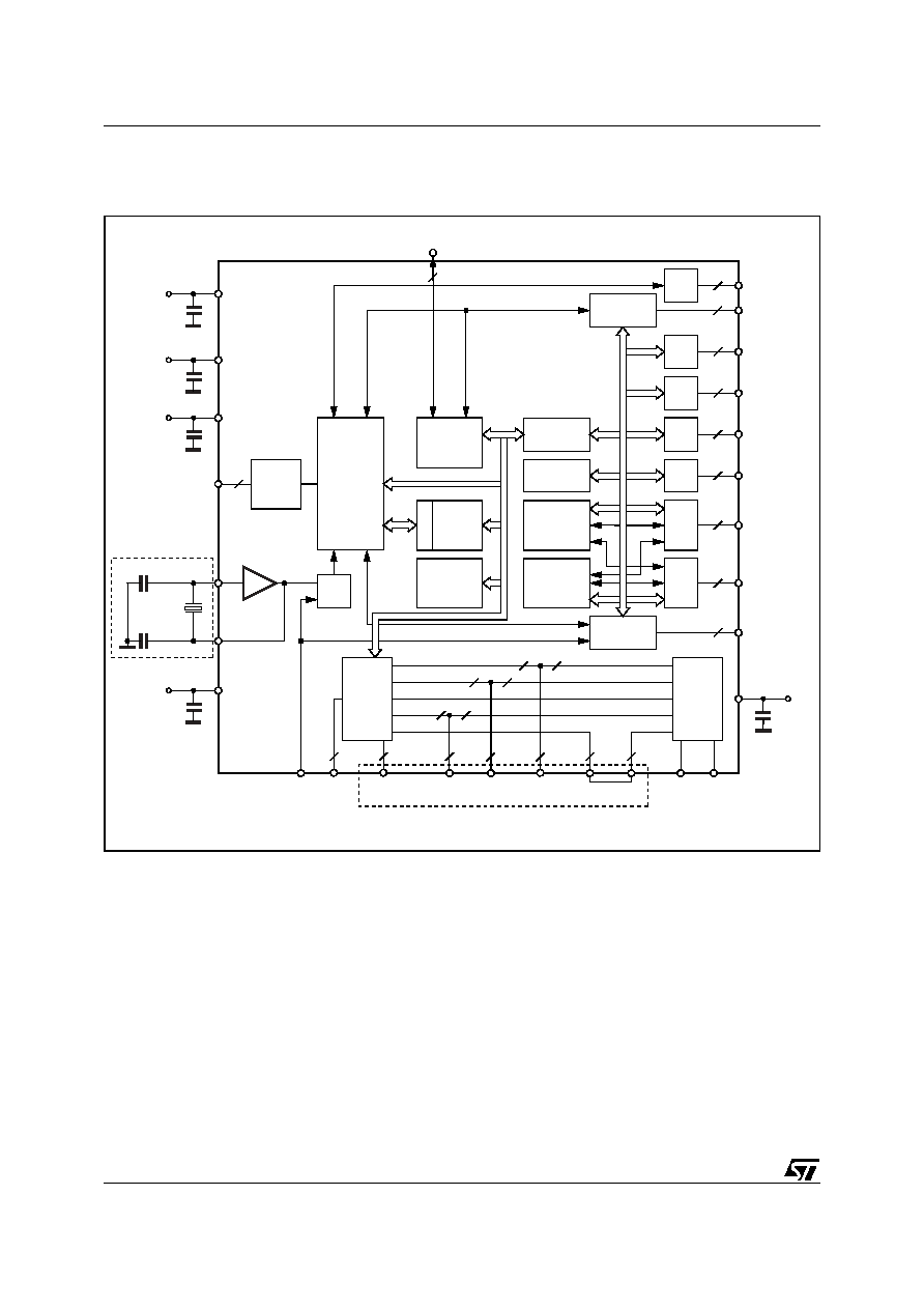
2
DESCRIPTION
The STLC2416 from STMicroelectronics is a BluetoothTM baseband controller with integrated 4 Mbit flash mem-
ory. Together with a BluetoothTM Radio this product offers a compact and complete solution for short-range wire-
less connectivity. It incorporates all the lower layer functions of the BluetoothTM protocol.
The microcontroller allows the support of all data packets of BluetoothTM in addition to voice. The embedded
controller can be used to run the BluetoothTM protocol and application layers if required. The software is located
in the integrated flash memory.
3
QUICK REFERENCE DATA
3.1 Absolute Maximum Ratings
Operation of the device beyond these conditions is not guaranteed.
Sustained exposure to these limits will adversely affect device reliability.
Table 2. Absolute Maximum Ratings
3.2 Operating Ranges
Operating ranges define the limits for functional operation and parametric characteristics of the device.
Functionality outside these limits is not implied.
Table 3. Operating Ranges
3.3 I/O specifications
Depending on the interface, the I/O voltage is typical 1.8V (interface to the flash memory) or typical 3.3V
(all the other interfaces). These I/Os comply with the EIA/JEDEC standard JESD8-B.
3.3.1
Specifications for 3.3V I/Os
Table 4. LVTTL DC Input Specification (3V<V
DDIO
<3.6V)
Symbol
Conditions
Min
Max
Unit
V
DD
Supply voltage baseband core
V
SS �
0.5
2.5
V
V
DDF
Supply voltage flash
V
SS �
0.5
2.5
V
V
PP
Fast Program Voltage
V
SS �
0.5
13
V
V
DDIO
Supply voltage baseband I/O
4
V
V
DDQ
Supply voltage flash I/O
V
SS �
0.5
2.5
V
V
IN
Input voltage on any digital pin (excluding FLASH input pins)
V
SS �
0.5
V
DDIO
+ 0.3
V
T
stg
Storage temperature
-55
+150
�C
T
lead
Lead temperature < 10s
+250
�C
Symbol
Conditions
Min
Typ
Max
Unit
V
DD
Supply voltage baseband core and EMI pads
1.55
1.8
1.95
V
V
DDF
Supply voltage flash
1.55
1.8
1.95
V
V
DDIO
Supply voltage digital I/O
2.7
3.3
3.6
V
V
DDQ
Supply voltage flash I/O (V
DDQ
V
DDF
)
1.55
1.8
1.95
V
T
amb
Operating ambient temperature
-40
+85
�C
Symbol
Parameter
Conditions
Min
Typ
Max
Unit
V
il
Low level input voltage
0.8
V
V
ih
High level input voltage
2
V
V
hyst
Schmitt trigger hysteresis
0.4
V
3/27
STLC2416
Table 5. LVTTL DC Output Specification (3V<V
DDIO
<3.6V)
Note: X is the source/sink current under worst-case conditions according to the drive capability. (See table 8, pad information for value of X).
3.3.2
Specifications for 1.8V I/Os
Table 6. DC Input Specification (1.55V<V
DD
<1.95V)
Table 7. DC Output Specification (1.55V<V
DD
<1.95V)
Note: X is the source/sink current under worst-case conditions according to the drive capability. (See table 8, pad information for value of X).
3.4 Current Consumption
Table 8. Typical power consumption of the STLC2416 (VDD = VDD Flash = PLLVDD = 1.8V, VDDIO = 3.3V)
(Indicative only)
Symbol
Parameter
Conditions
Min
Typ
Max
Unit
V
ol
Low level output voltage
I
ol
= X mA
0.15
V
V
oh
High level output voltage I
oh
=-X mA
V
DDIO
-0.15
V
Symbol
Parameter
Conditions
Min
Typ
Max
Unit
V
il
Low level input voltage
0.35*V
DD
V
V
ih
High level input voltage
0.65*V
DD
V
V
hyst
Schmitt trigger hysteresis
0.2
0.3
0.5
V
Symbol
Parameter
Conditions
Min
Typ
Max
Unit
V
ol
Low level output voltage
I
ol
= X mA
0.15
V
V
oh
High level output voltage
I
oh
=-X mA
V
DD
-0.15
V
STLC2416 State
Core
IO
Unit
Slave
Master
Standby (no low power mode)
5.10
5.10
0.13
mA
Standby (low power mode enabled)
0.94
0.94
0.13
mA
ACL connection (no transmission)
7.60
6.99
0.13
mA
ACL connection (data transmission)
7.90
7.20
0.13
mA
SCO connection (no codec connected)
8.70
7.90
0.14
mA
Inquiry and Page scan (low power mode enabled)
127
n.a.
5
�
A
Low Power mode (32 kHz crystal)
20
20
0
�A
5/27
STLC2416
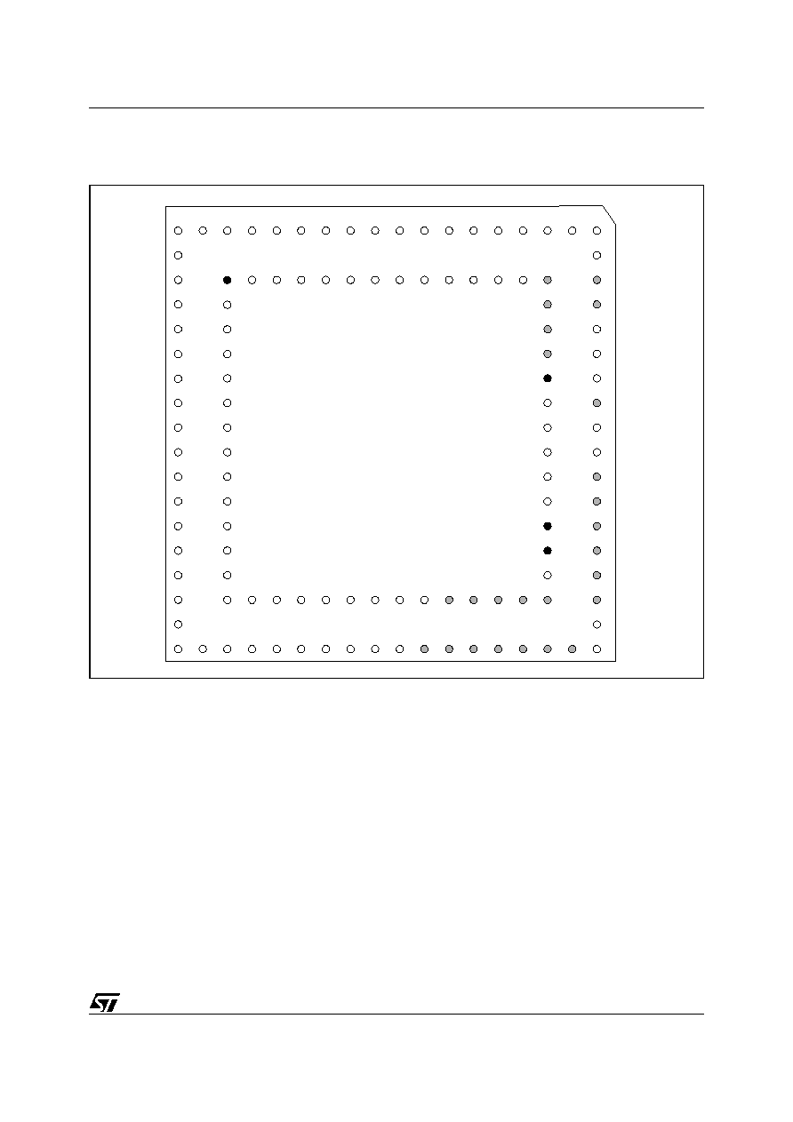
5
PINOUT
Figure 3. Pin out (Bottom view)
5.1 Pin Description and Assignment
Table 9 shows the pin list of the STLC2416. There are 91 functional pins of which 25 are used for device
testing only (should not be connected in the application) and 24 supply pins. The column "PU/PD" shows
the pads implementing an internal weak pull-up/down, to fix value if the pin is left open. This cannot re-
place an external pull-up/down.
The pads are grouped according to two different power supply values, as shown in column "VDD":
� V1 for 3.3 V typical 2.7 - 3.6 V range
� V2 for 1.8 V typical 1.55 - 1.95 V range
Finally the column "DIR" describes the pin directions:
� I for Inputs
� O for Outputs
� I/O for Input/Outputs
� O/t for tri-state outputs
D03TL583
A
B
C
D
E
F
G
H
J
K
L
M
N
P
R
T
U
V
14
13
12
11
18
17
16
15
10
9
8
7
6
5
4
3
2
1
i2c_
dat
i2c_
clk
pcm_
sync
pcm_
a
nreset
nrp
uart1_
rxd
uart1_
txd
usb_
dn
uart2_
rxd
uart2_
txd
uart2_
i1
uart2_
o2
vddio
vdd
vss
spi_
frm
spi_
clk
xin
int2
int1
vddio
n.c.
vssio
tck
vssio
tdo
tms
ntrst
tdi
btxen
ne
csn2
rdn/ng
csn1
addr0
vddio
sys_cl
k_req
brxen
addr2
nwp
vdd
vss
vpp
ant_sw
bpktcl
btxd
bpaen
bdclk
vddf
bmosi
brclk
vssf
addr17
vss
n.c.
vdd
pcm_
clk
pcm-
b
usb_
dp
uart2_
i2
uart2_
o1
uart2_
io1
uart2_
io2
vssio
brxd
bmiso
data3
data1
n.c.
n.c.
data0
addr19
vddq
csn0
spi_rxd
addr18
bsen
bnden
gpio3 gpio1
boot
vss
vdd
data8 data7 data6 data5 data4
gpio12
gpio14
gpio15
gpio10
gpio11
gpio13
gpio9
vddpll
gpio8 gpio7 gpio6
gpio2 gpio0
vddio
vsspll
gpio4
vssio
gpio5
lpo_
clk_n
lpo_
clk_p data15 data14 data13 data12 data11 data10 data9
data2
vss
vdd
spi_txd