 | –≠–ª–µ–∫—Ç—Ä–æ–Ω–Ω—ã–π –∫–æ–º–ø–æ–Ω–µ–Ω—Ç: STLC5432Q | –°–∫–∞—á–∞—Ç—å:  PDF PDF  ZIP ZIP |
STLC5432
2Mbit CEPT & PRIMARY RATE CONTROLLER DEVICE
PRELIMINARY DATA
ONE CHIP SOLUTION FROM PCM BUS TO
TRANSFORMER (CEPT STANDARD)
ISDN
PRIMARY
ACCESS
CONTROLLER
(COMPATIBLE WITH ETSI, OPTION 1 AND 2)
HDB3/BIN ENCODER AND DECODER ON
CHIP
MULTIFRAME STRUCTURE HANDLING
BUILT IN CRC4
EASY LINK TO ST5451/MK50H25/MK5027
LINK CONTROLLERS.
DATA RATE: 2048, 4096 AND 8192 Kb/s FOR
MULTIPLEXED APPLICATIONS
FOUR LOOPBACK MODES FOR TESTING
PSEUDO RANDOM SEQUENCE GENER-
ATOR AND ANALYZER FOR ON-LINE, OFF-
LINE AND AUTOTEST
CLOCK RECOVERY CIRCUITRY ON CHIP
64 BYTE ELASTIC MEMORY FOR TIME
COMPENSATION AND AUTOMATIC FRAME
AND SUPERFRAME ALIGNMENT
32 ON CHIP REGISTERS FOR CONFIGURA-
TIONS, TESTING, ALARMS, FAULT AND ER-
ROR RATE CONTROL.
AUTO ADAPTATIVE DETECTION THRESH-
OLD
AUTOMATIC EQUALIZER OPTION
5V POWER SUPPLY
AMI OR HDB3 CODE SELECTION
PARALLEL OR SERIAL MICROPROCESSOR
INTERFACE OPTION
BOTH
µ
p AND STAND ALONE MODE AVAIL-
ABLE
DESCRIPTION
STLC5432, CMOS device, interfaces the multi-
plex system to the physical CEPT Transmission
link at 2048Kb/s. Furthermore, thanks to its flexi-
bility, it is the optimum solution also for the ISDN
application as PRIMARY RATE CONTROLLER.
The receive circuit performances exceed CCITT
recommendation and the line driver outputs meet
the G.703 specifications.
STLC5432 is the real single chip solution that al-
lows the best system flexibility and easy design.
STLC5432 can work either in 2048 or 4096 or
8192 Kbit/s systems programming the CR4 regis-
ter (when parallel micro interface selected).
July 1996
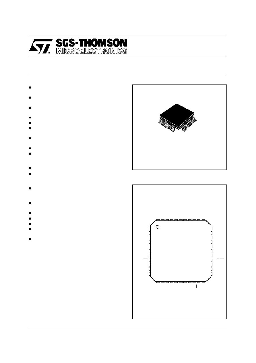
TQFP44 (10 x 10)
ORDERING NUMBER: STLC5432Q
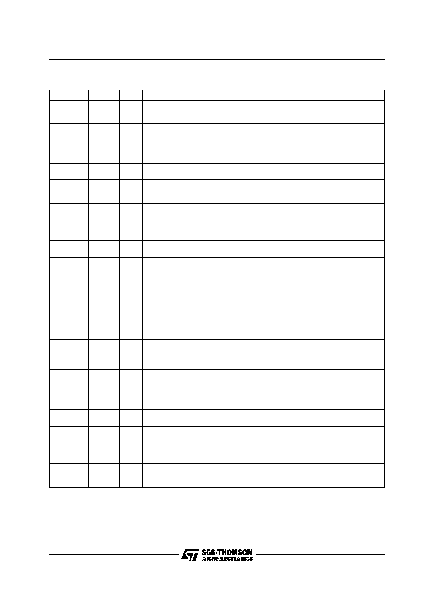
39
40
41
43
44
42
1
2
3
4
6
5
7
8
9
10
11
33
32
31
30
28
29
27
26
25
24
23
34
35
36
38 37
17
16
15
13
12
14
22
21
20
18 19
P0
LI1
VT
P1
GNDA
LI2
VCCA
CS
LO1
DPI
LO2
GNDD
SA/RESET
DIN
A/D0
A/D2
A/D1
A/D3
INT
RCLI
BRDI
DOUT
BXDI
AL0
AL1
A/D7
A/D5
A/D6
A/D4
R/W/WR
LFSX
LFSR
LCLK
VCCD2
XTAL2
XTAL1
AS/ALE
BRDO
RCLO
BXDO
DS/RD
LCR
VCCD1
HCR
D93TL043D
PIN CONNECTION (Top view)
1/46
PIN DESCRIPTION
Name
Pin
Type
Function
VCCD1
VCCD2
VCCA
18
17
34
I
I
I
Positive power supply inputs for the digital (V
CCD1
) and analog (V
CCA
) sections and for
microprocessor interface signals (V
CCD2
). They must be +5 Volts and must be directly
connected together.
GNDD
GNDA
1
44
I
I
Negative power supply pins which must be connected together close to the device. All
digital and analog signals are referred to these pins, which are normally at the system
ground.
LI1
LI2
40
42
I
I
Receive HDB3 signal differential inputs from the line transformer.
VT
41
O
Positive power supply output for fixing reference voltage to the receive transformer.
Typical value is 2.375V
L01
L02
36
37
O
O
Transmit HDB3 signal differential outputs to the line transformer.When used with an
appropriate transformer, the line signal conforms to the output specifications in CCITT
with a nominal pulse amplitude of 3 volts for a 120
load on line side.
XTAL1
15
I
The master clock input which requires either a parallel resonance crystal to be tied
between this pin and XTAL2, or a clock input from a stable source. This clock does
not need to be synchronized to the system clock.
Crystal specifications = 32764 kHz
±
50 ppm parallel resonant; RS
20
loaded with
33pF to GND each side.
XTAL2
16
O
The output of the crystal oscillator, which should be connected to one end of the
crystal if used.
HCR
19
O
High clock received, bit clock. When the device has recovered the clock from the
HDB3 signal, HCR signal is synchronized to the remote circuit. The HCR frequency is
either 8192kHz if 8MCR bit of CR1 Register is put to 1 or 4096 kHz if 8MCR is set to
0.
LCR
20
O
Low clock received, frame clock. When the device has recovered the clock from the
HDB3 signal, LCR signal is synchronized to the remote entity.
The LCR frequency is 8 kHz if 8KCR bit is set to 1, or 4 kHz if 8KCR bit is set to 0.
When the remote clock is not recovered, HCR and LCR frequency are synchronized
to master clock (16384 kHz).
HCR and LCR can be used by the system in Terminal Mode.These two clocks can be
used by the transmit function of the device.
BRDO
RCLO
12
14
O
O
Binary Receive Data Output, 2048 kbit/s or 64kbit/s.
Receive Clock output, 2048 kHz or 64kHz.
After decoding, Binary Data and clock associated are provided for different
applications.
BRDI
RCLI
10
9
I
I
Binary Receive Data Input. 2048 kbit/s.
Receive Clock Input 2048 kHz.
BXDO
22
O
Binary Transmit Data Output, 2048 kbit/s or output clock at 64kHz.
Before encoding Binary Data is provided to different applications (Optical Interface for
instance). Local clock is associated to this data.
BXDI
33
I
This binary signal can replace BXD internal signal to be encoded if SELEX bit (CR1
Register) is set to 1.
DOUT
11
O
Data Output. 30 B+D primary access data received from the line.Data can be shifted
out from the tristate output DOUT at the LCLK frequency on the rising edges during
all the time slots,except Time Slot Zero in accordance with TSOE bit (CR1Register).
NB : If parallel micro-interface is selected, DOUT is at high impedance after Reset.
DOUT is at low impedance after writing CR4 register.
DIN
3
I
Data Input : 30B+D primary access data to transmit to the line.Data can be shifted in
at the LCLK frequency on the falling edges during all the time slots, except Time Slot
Zero, in accordance with TSOE bit (CR1 Register).
STLC5432
2/46
PIN DESCRIPTION (continued)
Name
Pin
Type
Function
LCLK
23
I
Local Clock : this clock input determines the data shift rate on the two digital
multiplexes. This clock frequency can be indifferently 2048, 4096, 8192 or 16384kHz.
Data Out and Data In rate is always 2048 kbit/s when Serial Interface microprocessor:
an internal automatic mechanism divides by two the frequency if 4096 kHz.
LFSR
24
I
Local Frame Synchronization for the Receiver. This clock input defines the start of the
frame on the digital multiplex Data (pin DOUT). This clock frequency can be
indifferently 8 kHz or a submultiple of 8 kHz.
LFSX
25
I
Local Frame Synchronization for the Transmitter. This clock input defines the start of
the frame on the digital multiplex Data (pin DIN). This clock frequency can be
indifferently 8 kHz or a submultiple of 8 kHz.
If submultiple of 8 kHz, LFSX defines the start of even frame on DIN. The TSO of this
even frame will contain the Frame Alignment Signal (FAS) on the line.
AL0,
AL1
32
31
O
O
Alarm 0 Output, alarm 1 Output. These pins are open drain outputs which are
normally in high impedance state.
AL1
AL0
Alarm definitions
Z
Z
Frame or Multiframe recovered,
A bit received is 0.
0Volt
Z
Frame or Multiframe recovered,
A bit received is 1
Z
0Volt
Frame and Multiframe lost, AIS
Alarm Indication Signal is detected.
0Volt
0Volt
Frame and Multiframe lost, AIS
Alarm Indication Signal is not detected.
DPI
38
I
DPI input: The internal DPLL is synchronized either by the signal applied on DPI input
(if DPIS bit of CR5 register is = 0) or by the 2MHz clock recovered from the line.
SA/RESET
2
I
Stand Alone : When this pin is connected to 5 Volts, the device works without
microprocessor. The configuration is given by the values per default of programmable
registers. BRDI and BXDI must not be used.
RESET: When this pin is put to 5 Volts during 100 ns at least every programmable
register is reset (value per default). When this pin is set at zero Volt, the type of
microprocessor is selected by P0, P1 pins.
P0, P1
39, 43
I
Processor interface. These two input pins define the microprocessor interface
chosen.
P1
P0
Microprocessor Interface
-----------------------------------------------------------------------------------
0
0
Serial Microprocessor Interface
0
1
ST9 Microprocessor Interface
1
0
Multiplexed Motorola processor interface
1
1
Multiplexed Intel processor interface
AS/ALE
13
I
Address Strobe/Address Latch Enable. Input
CS
35
I
Chip Select. A high level on this input selects the PRCD for a read write operation.
R/W/WR
26
I
Read/Write/Write Data. Input.
DS/RD
21
I
Data Strobe/Read Data. Input.
A/D0 to A/D7
4 to 7;
27 to 30
I/O
Address/Data 0 to 7. Input-Output.
INT
8
O
Interrupt Request. The signal is activated low when the PRCD requests an interrupt. It
is an open drain output.
STLC5432
3/46

A
CLOCK
DATA
RECOVERY
HDB3/BIN
DECODER
LOOPBACK
1
LINE
DRIVER
PSEUDO
RANDOM
SEQUENCE
ANALYZER
From
A,
B
o
r
DIN
PSEUDO
RANDOM
SEQUENCE
GENERATOR
To
D
o
r
DOUT
LOOPBACK
3
LOOPBACK
2
ALARM
SIGNALS
BIN/HDB3
ENCODER
MULTIFRAME
GENERATION
LOOPBACK
4
64
BYTES
ELASTIC
MEMORY
SYNCHRONIZATION
AB
PROGRAMMABLE
REGISTERS
D
LFSR
DOUT
DIN
µ
P
INTERFACE
LFSX
BXDI
BXDO
RCLO
BRDO
BRDI
Q=32764KHz
2Mb/s
S2/T2
INTERFACE
D93TL044F
LCLK
64KHz
CLOCK
DPLL
LCR
HCR
RD+
RD-
BRD
BXD
BLOCK DIAGRAM
STLC5432
4/46

ABSOLUTE MAXIMUM RATINGS
Symbol
Parameter
Value
Unit
V
CC
to GND
Supply Voltage to Ground
7
V
V
I
Voltage at any digital or analog input
V
CC
+1 to GND-1
V
I
LO1
, I
OL2
Current at LO1 and LO2
±
100
mA
I
C
Current at any digital or analog input
±
30
mA
T
stg
Storage temperature range
-65 to +150
∞
C
T
L
Lead Temperature (soldering, 10s)
+300
∞
C
THERMAL DATA
Symbol
Parameter
Value
Unit
R
th j-amb
Thermal Resistance Junction to ambient
Max.
50
∞
C/W
ELECTRICAL CHARACTERISTICS (V
CC
= 5V
±
5%, T
amb
= 0 to 70
∞
C; Typical characteristics are speci-
fied at V
CC
= 5V, T
amb
= 25
∞
C; all signal are referenced to GND, unless otherwise specified.)
Symbol
Parameter
Test Condition
Min.
Typ.
Max.
Unit
DIGITAL INTERFACE
Vil
Input Low Voltage
All digital inputs
0.8
V
Vih
Input High Voltage
All digital inputs
2.2
V
Vilx
Input Low Voltage
XTAL1 input
0.5
V
Vihx
Input High Voltage
XTAL1 input
V
CC
-0.5
V
Vol
Output Low Voltage
I
L
= 7mA for pins AL0, AL1,
INT, DOUT, HCR, LCR.
All other digital outputs:
I
L
= 1mA
0.4
0.4
V
V
Voh
Output High Voltage
I
L
= 7mA for pins AL0, AL1,
INT, DOUT, HCR, LCR.
All other digital outputs:
I
L
= 1mA
2.4
2.4
V
V
Iil
Input Low Current
Any digital input, Gnd < Vin < Vil
10
µ
A
Iih
Input High Current
Any digital input, Gnd < Vin <
V
CC
10
µ
A
Ioz
Output Current in High
Impedance (tri-state)
All digital tri-state I/Os without
internal pull-up or pull-down
resistor.
10
µ
A
LINE INTERFACE FEATURES
Zin
Differential Input Resistance
DC measurement between LI1
and LI2 with the equalizer not
connected
200
K
Vin
Rx sensitivity
Relative to LI1/LI2 pins with
fixed detection threshold
0.6
Vpk
Vpk75
Transmit amplitude
75
at transformer secondary
2.14
2.37
2.60
Vpk
Vpk120
Transmit Amplitude
120
at transformer secondary
2.7
3
3.30
Vpk
Sym
Pulses Symetry
75
or 120
at transformer
secondary
5
%
Zero
Zero level
% nominal amplitude
10
%
Pwdth
Tx pulses width
at 50% of peak amplitude
219
244
269
ns
Zout
Differential Output Resistance
1
MASTERCLOCK
MCLK
MCLK Frequency
32.764
MHz
MCLK Frequency tolerance
≠50
50
ppm
JITTER PERFORMANCES (for jitter transfer function and admissible jitter please report to the corresponding
characteristics plotted in following page).
Intrinsic jitter
Filter 20Hz - 100KHz
0.125
UI
Intrinsic jitter
Filter 700Hz - 100KHz
0.12
UI
STLC5432
5/46