Æ
1/8
STLD20D
WHITE LED POWER SUPPLY
PRELIMINARY DATA
October 2004
REV. 2
FEATURES
High efficiency above 80%
Can drive up to 4 LEDs in series from 2.8V
supply
Constant LED current regulation
Integrated LED disconnect switch that cuts the
LEDs branch in shutdown mode
Constant switching frequency
Stable current regulation across the total input
voltage range
Supply voltage rejection
Inherent soft start by limiting the peak inductor
current
Peak inductor current adjustability (STLD20D-
C8 only)
Shutdown pin with possibility of PWM dimming
control
Over voltage and over temperature protection
with automatic restart
Low shutdown current < 1µA
Small external inductor (10µH, height < 2mm)
Tiny ceramic external capacitor
Can be supplied by a Li-ion battery - V
IN
range:
2.5Vdc to 5Vdc
Table 1: Order Codes
Part Number
Marking
Package
STLD20D-C8
L2D
SOT23-8L
STLD20D-DEF
L2D
QFN 3x3 8L
This is preliminary information on a new product now in development or undergoing evaluation. Details are subject to change without notice.
ASDTM
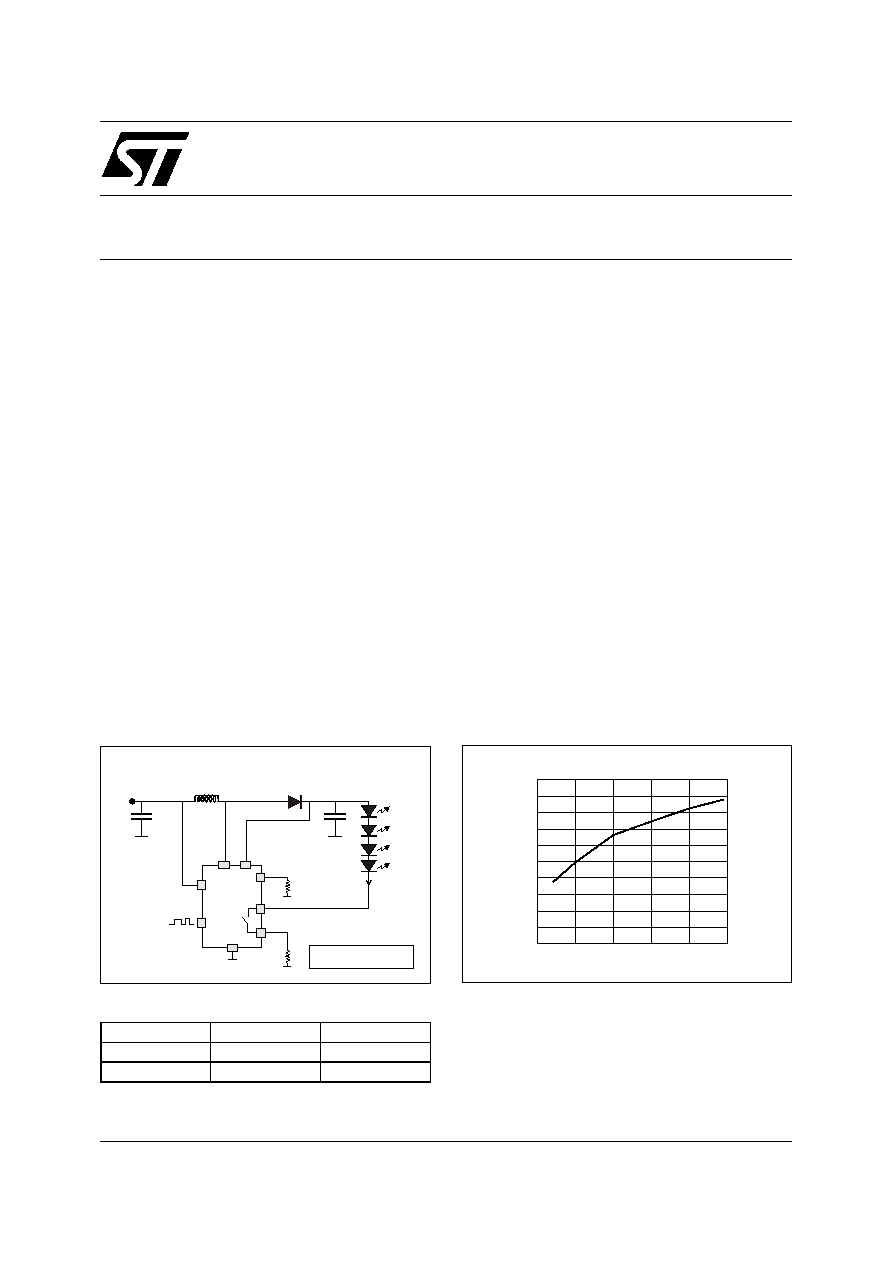
Figure 1: Basic connection
L = 10µH
D
Cout = 1µF
Cin = 2.2µF
I
= 20mA
LED
R
SET
V
BATT
R
LED
V
OUT
V
IN
LDS
FB
D: STM BAT20J
L: Murata LQH32CN100K33
SW
GND
(*) STLD20D-C8 only
SHDN
R
(*)
SET
STLD20D
APPLICATION
White Led supply for LCD backlight
Mobile phone
PDA and organizers
Any handsets powered from 2.8V to 4.2V
DESCRIPTION
The STLD20D is a constant switching frequency
boost regulator with specific features to supply up
to 4 white LEDs in series. A stable LED current
regulation, from 2.8V to 4.2V, is achieved by sens-
ing the LED current through a low ohmic shunt re-
sistor R
LED
(see figure 1). The device also
includes a supply rejection circuit that prevent any
kind of flickering effect on the display during dy-
namic supply voltage variation. A LED disconnect
switch cut the LED branch to reduce the current
consumption in shutdown mode. The maximum
peak inductor current can be programmed. The
STLD20D includes often numerous features and in-
novative design circuit that allows getting an efficien-
cy above 80% across the total supply voltage range.
Figure 2: Efficiency versus input voltage
(I
LED
=20mA; T
amb
=25∞C)
78
79
80
81
82
83
84
85
86
87
88
2.5
3
3.5
4
4.5
5
Input voltage (Vdc)
Efficiency (%)
STLD20D
2/8
Figure 5: Block Diagram
Figure 3: STLD20D-C8 Pin-Out Designation
(SOT23-8L top view)
Figure 4: STLD20D-DEF Pin-Out Designation
(QFN 8L top view)
SW
V
OUT
LDS
FB
FB
GND
V
IN
SHDN
R
SET
1
2
3
4
5
6
7
8
GND
V
IN
SHDN R
SET
FB
LDS
V
OUT
SW
GND
EXPOSED P
AD
SW
V
IN
V
OUT
SHDN
LDS
N/C
FB
1
2
3
4
5
6
7
8
GND
V
IN
SHDN
N/C
FB
LDS
V
OUT
SW
GND
SHDN
FB
V
IN
LDS
V
OUT
R
SET (*)
OSCILLATOR
OTP
OVP
RAMP
OSCILLATOR
COMPENSATION
PWN
COMP.
S
Q
R
+
+
+
-
-
-
POWER
FAULT
VIN
ENABLE
DRAIN
CURRENT
REFERENCE
LED DISCONNECT
LED CURRENT
REFERENCE
SHDN
VIN
SW
LDS
SW
(*) STLD20D-C8 only
T∞
V
IN
STLD20D
3/8
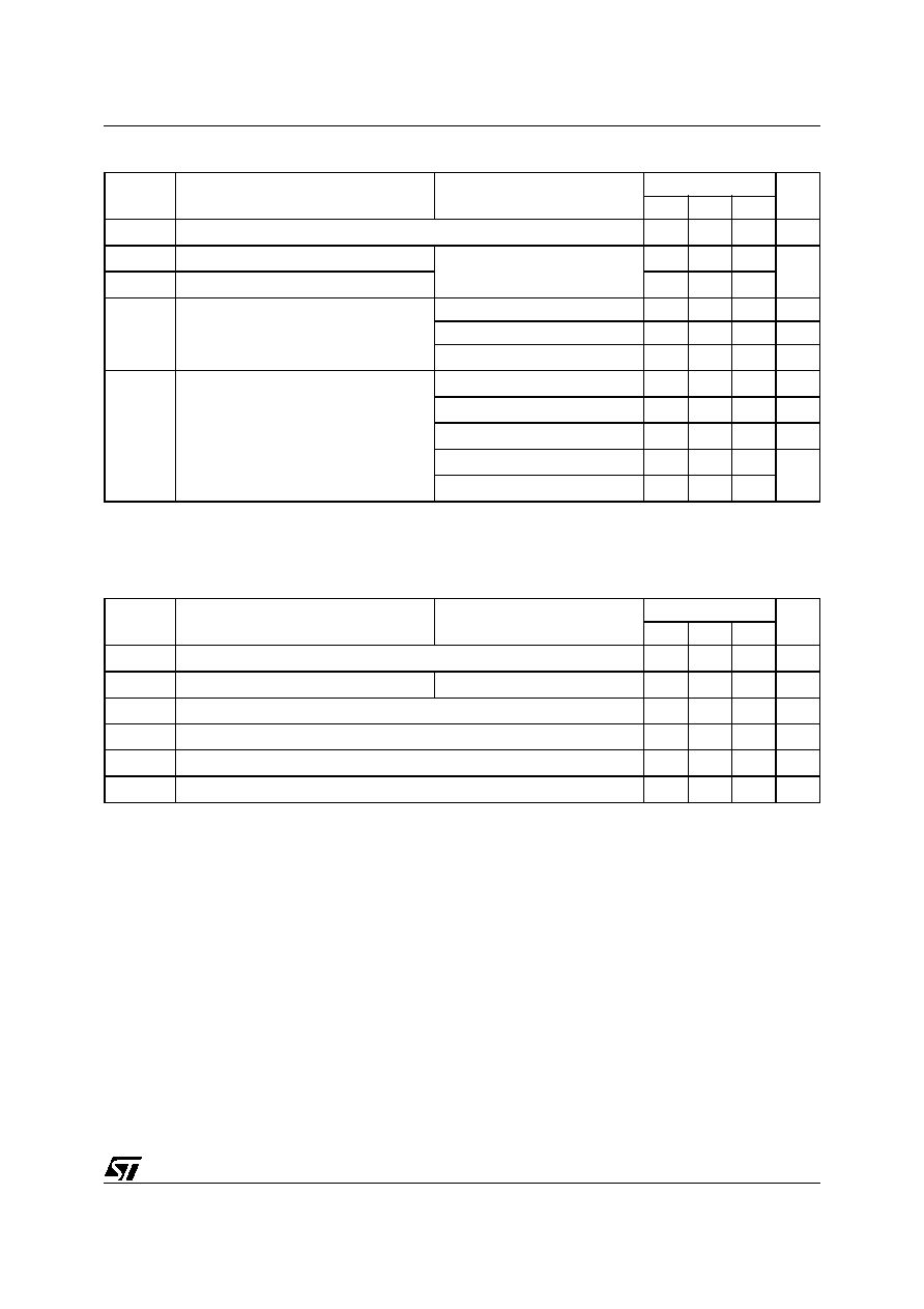
Table 2: External Components Pproposal
(note 1)
- Referred basic connection (figure 1)
Table 3: Absolute Maximum Ratings
Symbol
Parameter
Test Conditions
Value
Unit
Min. Typ. Max.
R
LED
LED current resistance
15
C
IN
Input filtering capacitor
Ceramic type
2.2
µF
C
OUT
Output capacitance
1
L
Boost inductor (height < 2mm)
Inductance
10
µH
Resistance at 500kHz
1
Isat (R
SET
= 100k
)
300
mA
D
Boost diode
(STMicroelectronics BAT20J type)
V
RRM
23
Vdc
I
F
(peak forward current)
1
A
V
F
@ I
F
= 0.1A Tj = 25∞C
0.35
0.4
V
I
R
@ Tj = 25∞C V
R
= 15V
3
12
µA
I
R
@ Tj = 85∞C V
R
= 15V
120
250
Note 1: the external components proposal should be considered as a design reference guide.
The performances mentioned in the electrical characteristics table are not guaranteed for all the possible electrical parameters of the com-
ponents included in this list. On an other hand the operation of STLD20D is not limited with the use of components included in this list.
Symbol
Parameter
Test conditions
Value
Unit
Min. Typ. Max.
V
IN
Supply voltage range
2.5
5
V
V
ESD
ESD ratings
HBM MIL STD 883C
2
kV
T
OP
Operating temperature
- 40
+ 85
∞C
T
stg
Storage temperature
- 65
150
∞C
B
VDS
Breakdown voltage at pin SW and TSS and V
OUT
20
V
SHDN
Maximum voltage applied on SHDN pin
V
IN
V
STLD20D
4/8
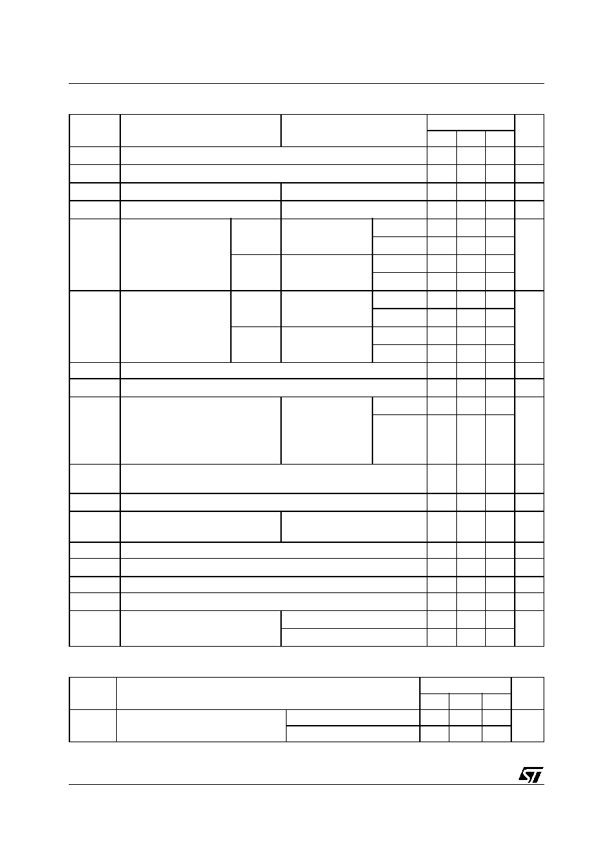
Table 4: Electrical Characteristics (for V
IN
= 2.8 to 4.2V and Tj = 25∞C)
Table 5: Thermal Characteristics
Symbol
Parameter
Test conditions
Value
Unit
Min. Typ. Max.
V
IN
Operating Input voltage range
2.8
4.2
V
I
OUT
Average regulated current I
OUT
= 20mA R
LED
= 15
19
20
21
mA
I
SD
Stand-by current
SHDN = low V
IN
= 4.2V
1
µA
I
Q
Quiescent current consumption
SHDN = high V
IN
= 4.2V
0.43
0.6
mA
SW
Boost switch RDSON
SOT23-8L Tj = 25∞C
I
SW
= 250mA
V
IN
= 2.8V
0.51
0.6
V
IN
= 4.2V
0.45 0.49
QFN
Tj = 25∞C
I
SW
= 250mA
V
IN
= 2.8V
0.65
V
IN
= 4.2V
0.55
LDS
Load disconnect switch
R
DSON
SOT23-8L Tj = 25∞C
I
LDS
= 20mA
V
IN
= 2.8V
5.5
6.1
V
IN
= 4.2V
4.7
5.2
QFN
Tj = 25∞C
I
LDS
= 20mA
V
IN
= 2.8V
6.2
V
IN
= 4.2V
5.3
FB
Feedback voltage
0.285 0.300 0.315
V
Line
Variation of the LED current versus the input voltage: R
LED
= 15
0.9 mA/V
Eff
Efficiency with 4 LEDS
Vout = 16V
Circuit configura-
tion (figure 1)
L: Murata
LQH32CN100K33
Diode: BAT20J
V
IN
= 2.8V
80
%
V
IN
= 4.2V
85
Switching
frequency
400
500
600
kHz
DC
MIN
Minimum duty cycle
22
25
%
I
LIM
Peak current boost switch
L = 10µH
R
SET
= GND (STLD20D-C8)
640
mA
OVP
Overvoltage protection
17.5 18.5
20
Vdc
Hyst
OV
Overvoltage hysteresis
0.7
Vdc
OTP
Over temperature protection
110
∞C
Hyst
OT
Over temperature protection hysteresis
5
∞C
SHDN
Shutdown signal logic
Disable Low V
IL
0.3
V
Enable high V
IH
1.2
Symbol
Parameter
Value
Unit
Min.
Typ. Max.
Rth(j-a)
Mounted on epoxy board without
copper heatsink
SOT23-8L
300
∞C/W
QFN
350
STLD20D
5/8
FUNCTIONAL DESCRIPTION
1. BOOST CONTROLLER:
The STLD20D is a PWM mode control boost con-
verter operating at 500kHz in discontinuous mode.
An automatic compensation of the oscillation ramp
allows rejection of the battery voltage transient. The
LED constant regulation (referred
figure 4
) is done
by sensing the LED current through the resistance
R
LED
(
figure 1
). The voltage across R
LED
is used by
the feedback loop of the controller (pin FB).
2. PEAK INDUCTOR CURRENT LIMITATION
AND SOFT START FUNCTION:
An integrated current sensor senses the peak drain current of the switch SW in order to keep the inductor
current below its saturation level. Since the peak drain current exceeds 590mA (if R
SET
= GND for
STLD20D-C8), the RS flip flop turns off the switch SW. During start up, this peak drain current limitation
acts inherently like a soft start function .
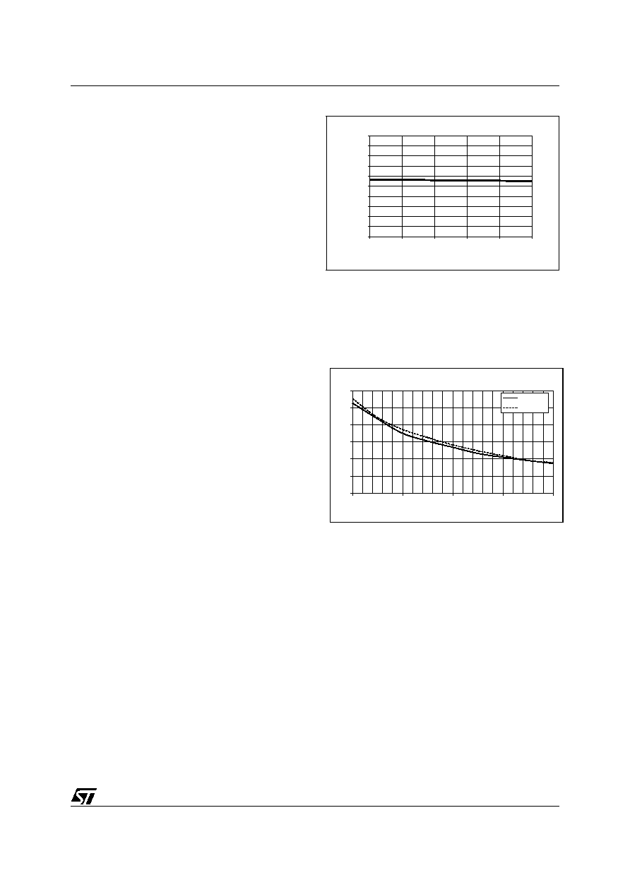
3. PEAK INDUCTOR CURRENT ADJUSTABILITY
(STLD20D-C8 ONLY)
The peak current of the boost inductor should always
be below the saturation current. In order to provide
flexibility in the selection of the inductor, the maxi-
mum peak inductor current can be adjusted by con-
necting a resistor at the pin R
SET
. The
figure 5
gives
the value of the resistance R
SET
versus the peak in-
ductor current limit I
LMAX
at 25∞C. If a low ripple is es-
pected on the battery voltage bus, then the
maximum peak inductor current should be reduced.
4. SHUTDOWN:
The SHDN pin is a low logic input signal and allows turning off the controller without cutting the input volt-
age from the boost regulator circuit. An integrated LED disconnect switch LDS disconnects the LEDs
branch in shutdown mode .This arrangement allows eliminating the DC current path that normally exists
with traditional boost regulator in shutdown mode.
5. BRIGHTNESS CONTROL:
The brightness of the Led is adjusted by pulsing the shutdown pin with a low frequency PWM signal.
By using such a PWM signal the controller is alternatively ON and OFF and the LED current changes from
full current to zero. The duty cycle allows to regulate the average LED current .
This scheme ensures that when the LEDs are ON they are driven at the full current without risk of color change.
6. OTP:
An integrated temperature sensor senses the temperature of the junction of the controller. when this tem-
perature exceeds 110∞C min fixed internally the controller is automatically turned OFF . When the tem-
perature is reduced the operation of the device automatically recovers.
Figure 6: LED current versus input voltage
V (V)
IN
I
(mA)
LED
19.00
19.20
19.40
19.60
19.80
20.00
20.20
20.40
20.60
20.80
21.00
2.5
3
3.5
4
4.5
5
Figure 7: R
SET
(k
) versus I
LMAX
(A)
I
(A)
Lmax
R
= f(I
)
SET
Lmax
R
(k )
SET
0
20
40
60
80
100
120
0.3
0.4
0.5
0.6
0.7
V =3.2V
IN
V =4.2V
IN