 | –≠–ª–µ–∫—Ç—Ä–æ–Ω–Ω—ã–π –∫–æ–º–ø–æ–Ω–µ–Ω—Ç: STLV3243E | –°–∫–∞—á–∞—Ç—å:  PDF PDF  ZIP ZIP |
Document Outline
- Table 1: Order Codes
- Table 2: Pin Description
- Figure 1: Pin Configuration
- Table 3: Invalid Truth Table
- Table 4: Output Control Truth Table
- Table 5: Absolute Maximum Ratings
- Table 6: ESD Performance: Transmitter Outputs, Receiver Inputs
- Table 7: Electrical Characteristics (C1 - C4 = 0.1mF, VCC = 2.3V to 5.5V, TA = -40 to 85�C, unles...
- Table 8: Logic Input Electrical Characteristics (C1 - C4 = 0.1mF, VCC = 2.3V to 5.5V, TA = -40 to...
- Table 9: Receiver Outputs Electrical Characteristics (C1 - C4 = 0.1mF, VCC = 2.3V to 5.5V, TA = -...
- Table 10: Auto-powerdown Electrical Characteristics (C1 - C4 = 0.1mF, VCC = 2.3V to 5.5V, TA = -4...
- Table 11: Transmitter Electrical Characteristics (C1 - C4 = 0.1mF, VCC = 2.3V to 5.5V, TA = -40 t...
- Table 12: Receiver Inputs Electrical Characteristics (C1 - C4 = 0.1mF, VCC = 2.3V to 5.5V, TA = -...
- Table 13: Timing Characteristics (C1 - C4 = 0.1mF, VCC = 2.3 to 3V, TA = -40 to 85�C, unless othe...
- Figure 2: Application Circuits
- Table 14: Required Minimum Capacitance Value (mF)
- Figure 3: Autopowerdown Input Levels
- Figure 4: Autopowerdown Input Timing
- Figure 5: Data Rate
- Table 15: Revision History
1/13
May 2005
I
ESD PROTECTION FOR RS-232 I/O PINS:
±8KV IEC 1000-4-2 CONTACT DISCHARGE
±15KV HUMAN BODY MODEL
I
1
µ
A SUPPLY CURRENT ACHIEVED WHEN
IN AUTO-POWERDOWN
I
250Kbps MINIMUM GUARANTEED DATA
RATE
I
GUARANTEED 6V/
µ
s SLEW RATE RANGE
I
GUARANTEED MOUSE DRIVEABILITY
I
0.1
µ
F EXTERNAL CAPACITORS
I
MEET EIA/TIA-562 SPECIFICATIONS
I
AVAILABLE IN FLIP-CHIP28 PACKAGES
DESCRIPTION
The STLV3243E device consists of 3 drivers, 5
receivers and a dual charge-pump circuit. All
transmitter outputs and receiver inputs are
protected up to ±8KV USING IEC 1000-4-2
contact discharge and ±15KV using the Human
Body Model. The receiver R2 is always active to
implement a wake-up feature for serial port. The
device is guaranteed to run at data rates of
250kbps while maintaining RS-562 output levels.
The Auto-powerdown feature operates when
FORCEON is low and FORCEOFF is high. During
this operation mode, if the device does not sense
a valid RS-562 signal, the driver outputs are
disabled. If FORCEOFF is set low, both drivers
and receivers (expert R2B) are shut off, and
supply current is reduced to 1
µ
A. Disconnecting
the serial port or turning off the peripheral drives
causes the auto-powerdown condition to occur.
Auto-powerdown can be disabled when
FORCEON and FORCEOFF are high, and this
should be done when driving a serial mouse. With
Auto-powerdown enabled, the device is
automatically activated when a valid signal is
applied to any receiver input.
Typical applications are notebooks, PDAs,
smart-phones, hand-held equipment, palmtop
computers, peripherals, battery-powered
equipment, and printers.
Table 1: Order Codes
Type
Temperature
Range
Package
Comments
STLV3243EBJR
-40 to 85 ∞C
FLIP-CHIP28 (6x5mm)
2500 parts per reel
STLV3243E
±15KV ESD PROTECTED 2.3 TO 5.5V, 400KBPS,
RS-232 TRANSCEIVER WITH AUTO-POWERDOWN
Flip-Chip28
Rev. 2
STLV3243E
2/13
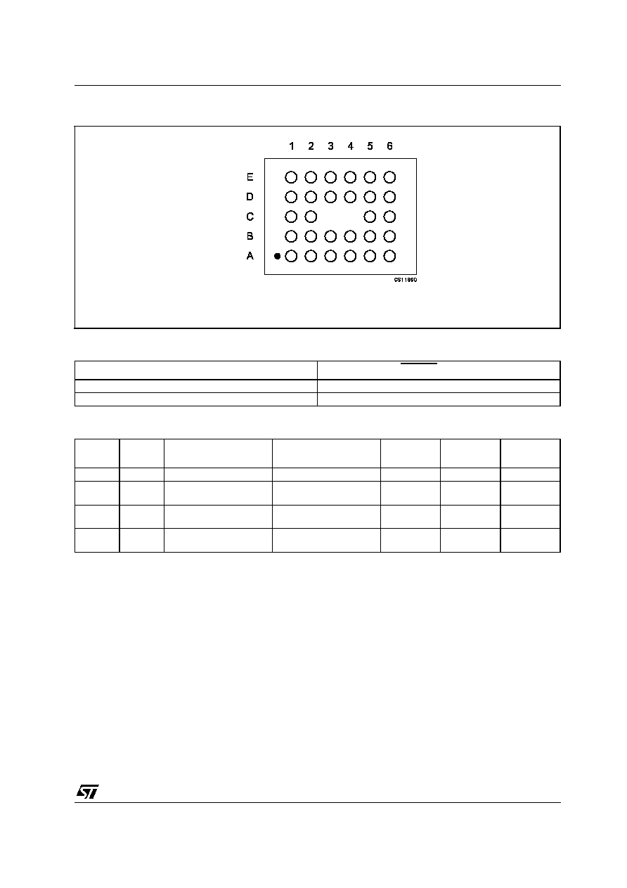
Table 2: Pin Description
PlN N∞
SYMBOL
NAME AND FUNCTION
A1
R2
IN
Second Receiver Input Voltage
A2
R3
IN
Third Receiver Input Voltage
A3
R4
IN
Fourth Receiver Input Voltage
A4
R5
IN
Fifth Receiver Input Voltage
A5
T1
OUT
First Transmitter Output Voltage
A6
T2
OUT
Second Transmitter Output Voltage
B1
V-
-5.5V Generated by the Charge Pump
B2
R1
IN
First Receiver Input Voltage
B3
T3
OUT
Third Transmitter Output Voltage
B4
T3
IN
Third Transmitter Input Voltage
B5
T1
IN
First Transmitter Input Voltage
B6
T2
IN
Second Transmitter Input Voltage
C1
C
2
+
Positive Terminal of Inverting Charge Pump Capacitor
C2
C
2
-
Negative Terminal of Inverting Charge Pump Capacitor
C5
R4
OUT
Fourth Receiver Output Voltage
C6
R5
OUT
Fifth Receiver Output Voltage
D1
C
1
+
Positive Terminal of Voltage- Charge Pump Capacitor
D2
V+
5.5V Generated by the Charge Pump
D3
V
CC
Supply Voltage
D4
FORCEON
Drive high to override automatic circuitry keeping transmitters
on (FORCEOFF must be high)
D5
R1
OUT
First Receiver Output Voltage
D6
R3
OUT
Third Receiver Output Voltage
E1
GND
Ground
E2
C
1
-
Negative Terminal of Voltage- Charge Pump Capacitor
E3
FORCEOFF
Drive low to shut down transmitters and on-board power
supply. This over-rides all automatic circuitry and FORCEON
E4
INVALID
Output of the valid signal detector. Indicates if a valid RS-232
level is present on receiver inputs logic "1"
E5
R2
OUTB
Non-inverting Complementary Receiver Output, always active
for wake-up
E6
R2
OUT
Second Receiver Output Voltage
STLV3243E
3/13
Figure 1: Pin Configuration
Table 3: Invalid Truth Table
Table 4: Output Control Truth Table
RS-232 SIGNAL PRESENT AT ANY RECEIVER INPUT
INVALID OUTPUT
YES
H
NO
L
FORCE
ON
FORCE
OFF
VALID RECEIVER
LEVEL
OPERATION STATUS
T
OUT
R
OUT
R
2OUTB
X
0
X
Shutdown (Force OFF)
HIGH Z
HIGH Z
ACTIVE
1
1
X
Normal Operating (Force
ON)
ACTIVE
ACTIVE
ACTIVE
0
1
YES
Normal Operating
(Auto-powerdown)
ACTIVE
ACTIVE
ACTIVE
0
1
NO
Shutdown (Auto-power-
down)
HIGH Z
ACTIVE
ACTIVE
FLIP-CHIP 6x5
(bottom view, bumps side)
STLV3243E
4/13
Table 5: Absolute Maximum Ratings
Absolute Maximum Ratings are those values beyond which damage to the device may occur. Functional operation under these condition is
not implied.
Table 6: ESD Performance: Transmitter Outputs, Receiver Inputs
Table 7: Electrical Characteristics
(C
1
- C
4
= 0.1
µ
F, V
CC
= 2.3V to 5.5V, T
A
= -40 to 85∞C, unless otherwise specified.
Typical values are referred to T
A
= 25∞C)
Table 8: Logic Input Electrical Characteristics
(C
1
- C
4
= 0.1
µ
F, V
CC
= 2.3V to 5.5V, T
A
= -40 to 85∞C, unless otherwise specified.
Typical values are referred to T
A
= 25∞C)
Symbol
Parameter
Value
Unit
V
CC
Supply Voltage
-0.3 to 6
V
V+
Doubled Voltage Terminal
(V
CC
-0.3) to 7
V
V-
Inverted Voltage Terminal
0.3 to -7
V
V+ +|V-|
13
V
FORCEON,
FORCEOFF,
T
IN
Input Voltage
-0.3 to 6
V
R
IN
Receiver Input Voltage Range
±
25
V
T
OUT
Transmitter Output Voltage Range
±
13.2
V
R
OUT
R
OUTB
INVALID
Receiver Output Voltage Range
-0.3 to (V
CC
+ 0.3)
V
t
SHORT
Short Circuit Duration on T
OUT
(one at a time)
Continuous
T
stg
Storage Temperature Range
-65 to 150
∞C
Symbol
Parameter
Test Conditions
Min.
Typ.
Max.
Unit
ESD
ESD Protection Voltage
Human Body Model
±
15
KV
ESD
ESD Protection Voltage
IEC 1000-4-2 (Contact Discharge)
±
8
KV
Symbol
Parameter
Test Conditions
Min.
Typ.
Max.
Unit
I
ASHDN
Supply Current
Auto-powerdown
FORCEOFF = GND
FORCEON = V
CC
All R_IN open or grounded
1
10
µ
A
I
SUPPLY
Supply Current
FORCEON = FORCEOFF = V
CC
0.3
1
mA
I
SHDN
Shutdown Supply Current
FORCEOFF = GND
1
10
µ
A
Symbol
Parameter
Test Conditions
Min.
Typ.
Max.
Unit
V
TIL
Input Logic Threshold Low
T-IN, FORCEON, FORCEOFF,
V
CC
= 3.0V
V
CC
= 2.3V
0.8
0.5
V
V
V
TIH
Input Logic Threshold High
T-IN, FORCEON, FORCEOFF
V
CC
= 3.0V
V
CC
= 2.3V
2
1.4
V
V
V
THYS
Transmitter Input
Hysteresis
0.4
V
I
IL
Input Leakage Current
T-IN, FORCEON, FORCEOFF
±
0.01
±
1.0
µ
A
STLV3243E
5/13
Table 9: Receiver Outputs Electrical Characteristics
(C
1
- C
4
= 0.1
µ
F, V
CC
= 2.3V to 5.5V, T
A
= -40 to 85∞C, unless otherwise specified.
Typical values are referred to T
A
= 25∞C)
Table 10: Auto-powerdown Electrical Characteristics
(C
1
- C
4
= 0.1
µ
F, V
CC
= 2.3V to 5.5V, T
A
= -40 to 85∞C, unless otherwise specified.
Typical values are referred to T
A
= 25∞C, FORCEON = GND, FORCEOFF = V
CC
)
Table 11: Transmitter Electrical Characteristics
(C
1
- C
4
= 0.1
µ
F, V
CC
= 2.3V to 5.5V, T
A
= -40 to 85∞C, unless otherwise specified.
Typical values are referred to T
A
= 25∞C)
Symbol
Parameter
Test Conditions
Min.
Typ.
Max.
Unit
I
OL
Output Leakage Current
Receiver Disabled
±
0.05
±
10
µ
A
V
OL
Output Voltage Low
I
OUT
= 1.6mA
0.4
V
V
OH
Output Voltage High
I
OUT
= -1mA
V
CC
-0.6 V
CC
-0.1
V
Symbol
Parameter
Test Conditions
Min.
Typ.
Max.
Unit
V
RITE
Receiver Input Threshold to
INVALID Output Voltage
HIGH (Fig. 1)
Positive Threshold
2.7
V
Negative Threshold
2.7
V
V
RITD
Receiver Input Threshold to
INVALID Output Voltage
LOW (Fig. 1)
-0.3
0.3
V
V
IOL
INVALID Output Voltage
LOW
I
OUT
= 1.6mA
0.4
V
V
IOH
INVALID Output Voltage
HIGH
I
OUT
= -1mA
V
CC
-0.6
V
t
WU
Receiver or Transmitter
Edge Transmitter Enabled
(Fig. 1)
100
µ
s
t
invh
Receiver Positive or
Negative Threshold to
INVALID HIGH (Fig. 1)
0.2
µ
s
t
invL
Receiver Positive or
Negative Threshold to
INVALID LOW (Fig. 1)
30
µ
s
Symbol
Parameter
Test Conditions
Min.
Typ.
Max.
Unit
V
TOUT
Output Voltage Swing
All Transmitter outputs are loaded with
3K
to GND
V
CC
= 3.0V
V
CC
= 2.3V
±
3.7
±
4.4
±
3.9
V
R
OUT
Output Resistance
V
CC
= V+ = V- = 0V
V
OUT
=
±
2V
300
10M
I
SC
Output Short Circuit Current V
CC
= 3.3V
±
40
±
60
mA
I
L
Output Leakage Current
V
CC
= 0 to 5.5V, transmitter output =±12V,
transmitter disabled
±
25
mA
V
OT
Transmitter Output Voltage
T1IN = T2IN = GND,
T3IN = V
CC
T3OUT loaded with 3K
to GND
T1OUT and T2OUT loaded with 2.5mA
each
±
3.7
V