1/12
December 2002
s
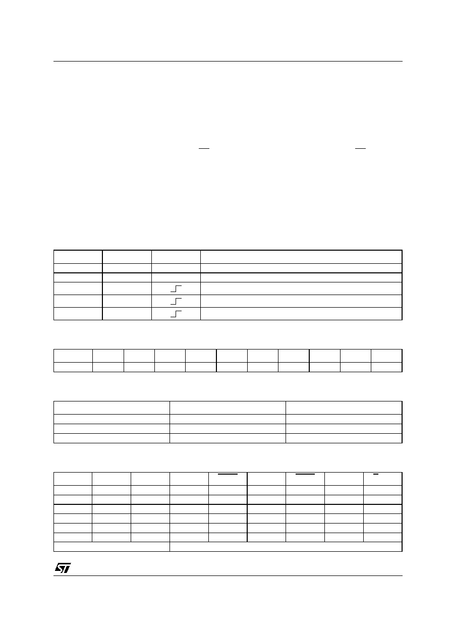
100ps PART-TO PART SKEW
s
50ps BANK SKEW
s
DIFFERENTIAL DESIGN
s
MEETS LVDS SPEC. FOR DRIVER
OUTPUTS AND RECEIVER INPUTS
s
REFERENCE VOLTAGE AVAILABLE
OUTPUT V
BB
s
LOW VOLTAGE V
CC
RANGE OF 2.375V TO
2.625V
s
HIGH SIGNALLING RATE CAPABILITY
(EXCEEDS 622MHz)
s
SUPPORT OPEN, SHORT AND
TERMINATED INPUT FAIL-SAFE (LOW
OUTPUT STATE)
s
PROGRAMMABLE DRIVERS POWER OFF
CONTROL
DESCRIPTION
The STLVD111 is a low skew programmable 1 to
10 differential LVDS driver, designed for clock
distribution. The select signal is fanned out to 10
identical differential outputs.
The STLVD111 is provided with a 11 bit shift
register with a serial in and a Control Register.
The purpose is to enable or power off each output
clock channel and to select the clock input. The
STLVD111 is specifically designed, modelled and
produced with low skew as the key goal. Optimal
design and layout serve to minimize gate to gate
skew within a device. The net result is a
dependable guaranteed low skew device.
The STLVD111 can be used for high performance
clock distribution in 2.5V systems with LVDS
levels. Designers can take advantage of the
device's performance to distribute low skew
clocks across the backplane or the board.
ORDERING CODES
Type
Temperature
Range
Package
Comments
STLVD111BF
-40 to 85 �C
TQFP32 (Tray)
250 parts per Tray
STLVD111BFR
-40 to 85 �C
TQFP32 (Tape & Reel)
2400 parts per reel
STLVD111
PROGRAMMABLE LOW VOLTAGE
1:10 DIFFERENTIAL LVDS CLOCK DRIVER
TQFP32
STLVD111
2/12
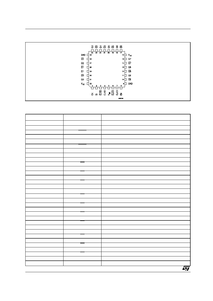
PIN CONFIGURATION
PIN DESCRIPTION
PlN N�
SYMBOL
NAME AND FUNCTION
1
CK
Control Register Clock
2
SI
Control Register Serial IN/CLK_SEL
3
CLK0
Differential Input
4
CLK0
Differential Input
5
V
BB
Output Reference Voltage
6
CLK1
Differential Input
7
CLK1
Differential Input
8
EN
Device Enable/Program
9
GND
Ground
10
Q9
Differential Outputs
11
Q9
Differential Outputs
12
Q8
Differential Outputs
13
Q8
Differential Outputs
14
Q7
Differential Outputs
15
Q7
Differential Outputs
16
V
CC
Supply Voltage
17
Q6
Differential Outputs
18
Q6
Differential Outputs
19
Q5
Differential Outputs
20
Q5
Differential Outputs
21
Q4
Differential Outputs
22
Q4
Differential Outputs
23
Q3
Differential Outputs
24
Q3
Differential Outputs
25
GND
Ground
26
Q2
Differential Outputs
27
Q2
Differential Outputs
28
Q1
Differential Outputs
29
Q1
Differential Outputs
30
Q0
Differential Outputs
31
Q0
Differential Outputs
32
V
CC
Supply Voltage
STLVD111
3/12
ABSOLUTE MAXIMUM RATINGS
Absolute Maximum Ratings are those values beyond which damage to the device may occur. Functional operation under these condition is
not implied.
THERMAL DATA
RECOMMENDED OPERATING CONDITIONS
DRIVER ELECTRICAL CHARACTERISTICS (T
A
= -40 to 85 �C, V
CC
= 2.5V � 5%, unless otherwise
specified (Note 1, 2)
NOTE 1: All currents into device pins are positive; all currents out of device pins are negative. All voltages are referenced to device ground
unless otherwise specified.
NOTE 2: All typical values are given for V
CC
= 2.5V and T
A
= 25�C unless otherwise stated.
RECEIVER ELECTRICAL CHARACTERISTICS (T
A
= -40 to 85 �C, V
CC
= 2.5V � 5%, unless otherwise
specified (Note 1, 2)
NOTE 1: All currents into device pins are positive; all currents out of device pins are negative. All voltages are referenced to device ground
unless otherwise specified.
NOTE 2: All typical values are given for V
CC
= 2.5V and T
A
= 25�C unless otherwise stated.
Symbol
Parameter
Value
Unit
V
CC
Supply Voltage
-0.3 to 2.8
V
V
I
Input Voltage
-0.2 to (V
CC
+0.2)
V
V
O
Output Voltage
-0.2 to (V
CC
+0.2)
V
I
OSD
Driver Short Circuit Current
Continuous
ESD
Electrostatic Discharge (HBM 1.5K
,
100pF)
>2
KV
Symbol
Parameter
Value
Unit
R
Tj-c
Thermal Resistance Junction-Case
13
�C/W
Symbol
Parameter
Min
TYP
Max
Unit
V
CC
Supply Voltage
2.375
2.625
V
V
IC
Receiver Common Mode Input Voltage
0.5(V
ID
)
2-0.5(V
ID
)
V
T
A
Operating Free-Air Temperature Range
-40
85
�C
T
J
Operating Junction Temperature
-40
105
�C
Symbol
Parameter
Test Conditions
Value
Unit
Min.
Typ.
Max.
V
OD
Output Differential Voltage
(Fig. 2)
R
L
= 100
400
500
600
mV
V
OD
V
OD
Magnitude Change
30
mV
V
OS
Offset Voltage
-40
T
A
85�C
1.05
1.15
1.25
V
V
OS
V
OS
Magnitude Change
30
V
I
OS
Output Short Circuit Current V
O
= 0V
15
30
mA
V
OD
= 0V
7
15
Symbol
Parameter
Test Conditions
Value
Unit
Min.
Typ.
Max.
V
IDH
Input Threshold High
100
mV
V
IDL
Input Threshold Low
-100
mV
I
IN
Input Current
V
I
= 0V
42
100
�
A
V
I
= 0V
CC
2
10
STLVD111
4/12
DRIVER ELECTRICAL CHARACTERISTICS (T
A
= -40 to 85 �C, V
CC
= 2.5V � 5%, unless otherwise
specified (Note 1, 2)
NOTE 1: All currents into device pins are positive; all currents out of device pins are negative. All voltages are referenced to device ground
unless otherwise specified.
NOTE 2: All typical values are given for V
CC
= 2.5V and T
A
= 25�C unless otherwise stated.
LVDS TIMING CHARACTERISTICS (T
A
= -40 to 85 �C, V
CC
= 2.5V � 5%, unless otherwise specified
(Note 4)
NOTE 4: Generator waveforms for all test conditions: f=1MHz, Z
O
= 50
(unless otherwise specified).
CONTROL REGISTER TIMING CHARACTERISTICS (T
A
= -40 to 85 �C, V
CC
= 2.5V � 5%, EN=H, unless
otherwise specified (Figure 4)
Symbol
Parameter
Test Conditions
Value
Unit
Min.
Typ.
Max.
V
BB
Output Reference Voltage
V
CC
= 2.5 V
1.15
1.25
1.35
V
I
CCD
Power Supply Current
All driver enabled and loaded
125
160
mA
C
IN
Input Capacitance
V
I
= 0V to V
CC
5
pF
C
OUT
Output Capacitance
5
pF
V
IH
Logic Input High Threshold
V
CC
= 2.5 V
2
V
V
IL
Logic Input Low Threshold
V
CC
= 2.5 V
0.8
V
I
I
Logic Input Current
V
CC
= 2.5 V,
V
IN
= V
CC
or GND
�10
�A
Symbol
Parameter
Test Conditions
Value
Unit
Min.
Typ.
Max.
t
TLH,
t
THL
Transition Time
R
L
= 100
, C
L
= 5 pF, Fig. 5, 6)
220
300
ps
t
PHL,
t
PLH
Propagation Delay Time
(Fig. 5, 6)
2
2.5
ns
f
MAX
Maximum Input Frequency
700
900
MHz
t
SKEW
Bank Skew
(Fig. 1)
50
ps
Part to Part Skew
(Fig. 2)
100
Pulse Skew
(Fig. 3)
50
Symbol
Parameter
Test Conditions
Value
Unit
Min.
Typ.
Max.
f
MAX
Maximum Frequency of Shift
Register
(Fig. 7)
100
150
MHz
t
s
Clock to SI Setup Time
(Fig. 7)
2
ns
t
h
Clock to SI Hold Time
(Fig. 7)
1.5
ns
t
rem
Enable to Clock Removal Time
(Fig. 7)
1.5
ns
t
W
Minimum Clock Pulse Width
(Fig. 7)
3
ns
STLVD111
5/12
SPECIFICATION OF CONTROL REGISTER
The STLVD111 is provided with a 11 bit shift register with a Serial In and a Control Register. The purpose
is to enable or power of each output clock channel and to select the clock input. The STLVD111 provides
two working modality:
PROGRAMMED MODE (EN=1)
The shift register have a serial input to load the working configuration. Once the configuration is loaded
with 11 clock pulse, another clock pulse load the configuration into the control register. The first bit on the
serial input line enables the outputs Q9 and Q9, the second bit enables the outputs Q8 and Q8 and so on.
The last bit is the clock selection bit. To restart the configuration of the shift register a reset of the state
machine must be done with a clock pulse on CK and the EN set to Low. The control register shift register
can be configured on time after each reset.
STANDARD MODE (EN=0)
In Standard Mode the STLVD111 isn't programmable, all the clock outputs are enabled. The LVDS clock
input is selected from Clock 0 or Clock 1 with the SI pin as shown in the Truth Table below.
TRUTH TABLE OF STATE MACHINE INPUTS
SERIAL INPUT SEQUENCE
TRUTH TABLE OF THE CONTROL REGISTER
TRUTH TABLE
EN
SI
CK
OUTPUT
L
L
X
All Output Enabled, Clock 0 selected, Control Register disabled
L
H
X
All Output Enabled, Clock 1 selected, Control Register disabled
H
L
First stage stores "L", other stages store the data of previous stage
H
H
First stage stores "H", other stages store the data of previous stage
L
X
Reset of the state machine, Shift register and Control Register
BIT#10
BIT#9
BIT#8
BIT#7
BIT#6
BIT#5
BIT#4
BIT#3
BIT#2
BIT#1
BIT#0
CLK_SEL
Q0
Q1
Q2
Q3
Q4
Q5
Q6
Q7
Q8
Q9
BIT#10
BIT#(0-9)
Qn(0-9)
L
H
Clock 0
H
H
Clock 1
X
L
Qn Output Disabled
CK
EN
SI
CLK 0
CLK 0
CLK 1
CLK 1
Q (0-9)
Q(0-9)
L
L
L
L
H
X
X
L
H
L
L
L
H
L
X
X
H
L
L
L
L
Open
Open
X
X
L
H
L
L
H
X
X
L
H
L
H
L
L
H
X
X
H
L
H
L
L
L
H
X
X
Open
Open
L
H
All drivers enable