1/11
April 2003
s
24mA CMOS OUTPUT DRIVE CURRENT
s
LVTTL INPUT THRESHOLDS
s
CONTROLLED SKEW BETWEEN DATA AND
CLOCK SIGNALS
s
LVDS INPUT-OUTPUT UP TO 155 MHZ
s
IMPROVED LATCH-UP IMMUNITY UP TO
300mA
DESCRIPTION
The STLVD112 is a low voltage differential to
LVTTL signal converter with enhanced loop-back
and crosspoint features. The synchronous design
allows a phase alignment between a clock and its
data; this means a better BER (Bit Error Rate)
performance.
The advanced 0.35µm technology makes the
STLVD112 suitable for data rates up to 200Mbit.
The main application field is SDH/SONET telecom
infrastructure. The STLVD112 flexible switch
architecture makes it easy to implement multiple
protection schemes in STM1 access systems.
Thanks to the flexible multiplexing allowed, it
becomes simple to redirect the data/clock signal
coming from the faulty access card to the spare
card. In normal mode the STLVD112 converts the
differential data levels of the LVDS and related
clock signal from (to) the line interface in LVTTL
level signals to (from) the backpanel. In addition
the switch functions prevent the equipment from
line interface faults. In fact, it is possible to switch
the signals coming from a different line interface to
the local line interface or the signals from the local
line interface to a different line interface.
ORDERING CODES
Type
Temperature
Range
Package
Comments
STLVD112BTR
-40 to 85 ∞C
TSSOP48 (Tape & Reel)
1000 parts per reel
STLVD112CTR
0 to 70 ∞C
TSSOP48 (Tape & Reel)
1000 parts per reel
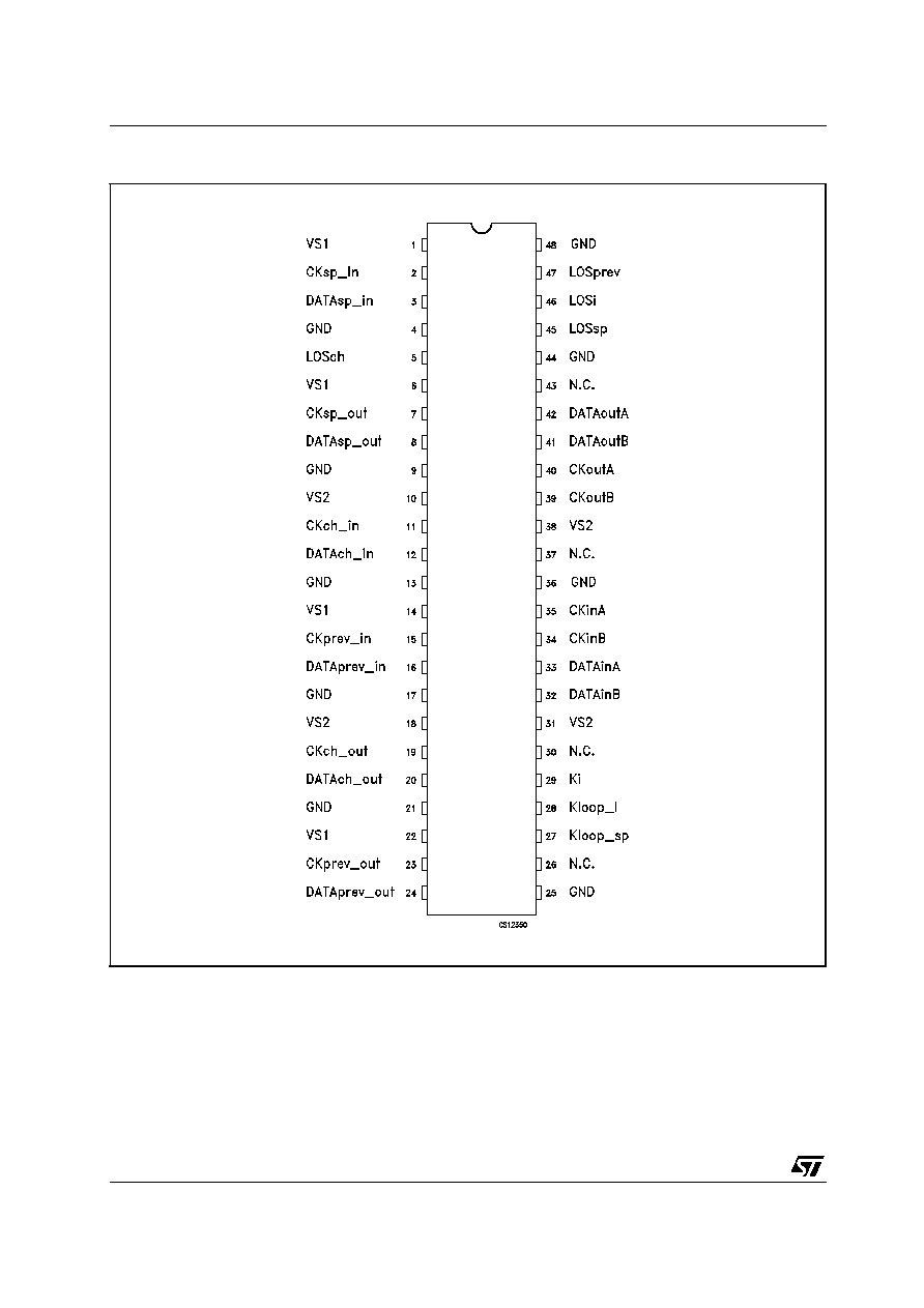
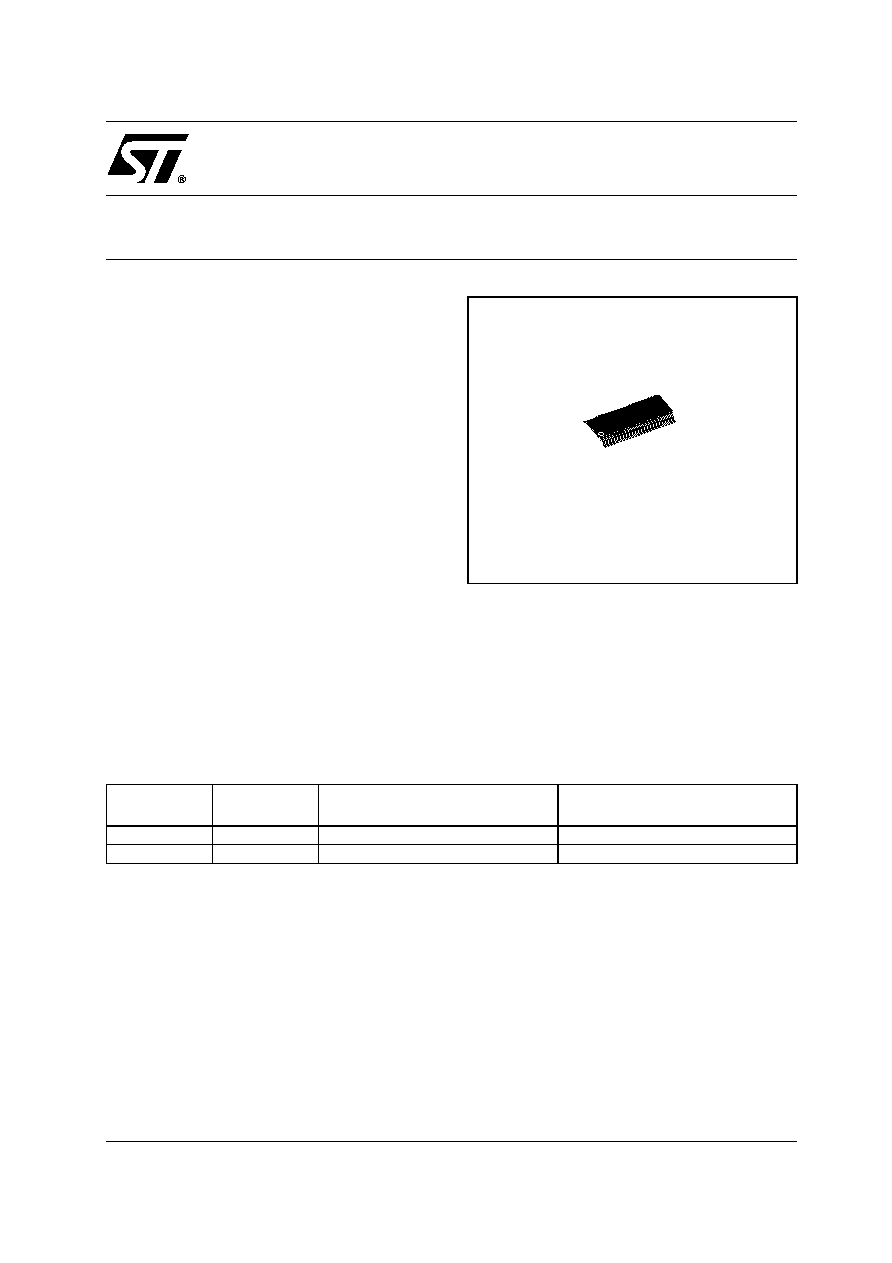
STLVD112
HIGH SPEED PROTECTION SWITCH
TSSOP
STLVD112
4/11
ABSOLUTE MAXIMUM RATINGS
Absolute Maximum Ratings are those values beyond which damage to the device may occur. Functional operation under these conditions is
not implied.
RECOMMENDED OPERATING CONDITIONS
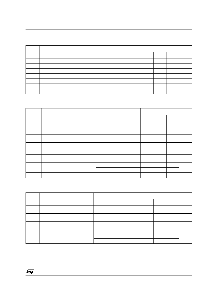
INPUTS
OUTPUT
Ki
Kloop_sp
Kloop_i
DATAsp_out
LOW
LOW
X
DATAprev_in
HIGH
LOW
X
DATA_in
X
HIGH
X
DATAsp_in
INPUTS
OUTPUT
Ki
Kloop_sp
Kloop_i
LOSch
X
X
LOW
LOSi
X
X
HIGH
LOW
INPUTS
OUTPUT
Ki
Kloop_sp
Kloop_i
LOSsp
LOW
LOW
X
LOSprev
HIGH
LOW
X
LOSi
X
HIGH
X
LOW
Symbol
Parameter
Value
Unit
VS1, VS2
Supply Voltage
-0.3 to 4.6
V
VS2
Supply Voltage
-0.3 to (VS1 + 0.3)
V
V
I
DC Input Voltage
-0.3 to (VS1 + 0.3)
V
V
O
DC Output Voltage
-0.3 to (VS1 + 0.3)
V
Iik
DC Input Diode Clamp Current
±20
mA
Iok
DC Output Diode Clamp Current
±20
mA
I
O
DC Output Current
±50
mA
T
L
Lead Temperature (10sec)
300
∞C
T
stg
Storage Temperature Range
-65 to 150
∞C
Symbol
Parameter
Value
Unit
VS1, VS2
Supply Voltage
3 to 3.6
V
VS2
Supply Voltage
3 to (VS1 + 0.3)
V
V
I
DC Input Voltage
0 to VS1
V
V
O
DC Output Voltage
0 to VS1
V
Top
Operating Temperature
-45 to 85
∞C
dt/dv
Maximum Input Rise and Fall Time
10
ns/V
STLVD112
5/11
ELECTRICAL CHARACTERISTICS (Over recommended operating conditions, unless otherwise noted.
All typical values are at T
A
=25∞C and V
S1
, V
S2
= 3.3V)
LVDS DRIVER ELECTRICAL CHARACTERISTICS (Over recommended operating conditions, unless
otherwise noted. All typical values are at T
A
=25∞C and V
S1
, V
S2
= 3.3V)
LVDS RECEIVER ELECTRICAL CHARACTERISTICS (Over recommended operating conditions,
unless otherwise noted. All typical values are at T
A
=25∞C and V
S1
, V
S2
= 3.3V)
Symbol
Parameter
Test Conditions
Value
Unit
Min.
Typ.
Max.
V
OL
Low Level Output Voltage
I
OUT
= 24 mA
0.2
0.4
V
V
OH
High Level Output Voltage
I
OUT
= 24 mA
V
SI
-0.5
V
SI
-0.3
V
V
IL
Low Level Input Thresholds V
OUT
= 0.1V or V
S1
- 0.1
0
0.8
V
V
IH
High Level Input Thresholds V
OUT
= 0.1V or V
S1
- 0.1
2
V
SI
V
I
IN
Input Leakage Current
V
IN
= GND or V
CC
-1
1
µA
I
CC
Quiescent Supply Current
V
IN
= GND or V
CC
15
mA
f
CLOCK
= 155MHz
110
Symbol
Parameter
Test Conditions
Value
Unit
Min.
Typ.
Max.
V
OD
Differential Output Voltage
R
L
= 100
247
364
454
mV
V
OD
Change in differential output voltage
between logic states
-50
50
mV
V
OC(SS)
Steady-state common-mode output
voltage
1
1.15
1.30
V
V
OC(SS)
Change in steady-state common-
mode output voltage between logic
State
-50
50
mV
V
OC(PP)
Peak-to-Peack common-mode output
voltage
100
150
mV
I
SC
Short Circuit Output Current
V
O(Y)
or V
O(Z)
= 0
-24
-4
mA
V
OD
= 0
±12
I
OFF
Power Off Output Current
V
CC
= 0, V
O
= 2.4V
-1
1
µA
Symbol
Parameter
Test Conditions
Value
Unit
Min.
Typ.
Max.
V
ITH+
Positive-going Differential Input
Voltage Threshold
100
mV
V
ITH-
Negative-going Differential Input
Voltage Threshold
-100
mV
|V
ID
|
Magnitude of Differential Input
Voltage
0.1
0.6
V
V
IC
Common-mode Input Voltage
0.5
|V
ID
|
2.4-0.5
|V
ID
|
V
V
CC
-1