 | –≠–ª–µ–∫—Ç—Ä–æ–Ω–Ω—ã–π –∫–æ–º–ø–æ–Ω–µ–Ω—Ç: STM1404C | –°–∫–∞—á–∞—Ç—å:  PDF PDF  ZIP ZIP |
1/9
DATA BRIEFING
January 2006
For further information contact your local ST sales office.
STM1404
3V FIPS-140
Security Supervisor with Battery Switchover
Rev 4.0
FEATURES
STM1404 SUPPORTS FIPS-140 SECURITY
LEVEL 4
≠
4 High-Impedance Physical Tamper
Inputs
≠
Over/Under Operating Voltage Detector
≠
Security Alarm (SAL) on Tamper
Detection
≠
Over/Under Operating Temperature
Detector
≠
Over/Under Temperature Thresholds are
Customer-Selectable and Factory-
Programmed
SUPERVISORY FUNCTIONS
≠
Automatic Battery Switchover
≠
RST Output (Open Drain)
≠
Manual (Push-button) Reset Input (MR)
≠
Power-fail Comparator (PFI/PFO)
Vccsw (V
CC
SWITCH OUTPUT)
≠
Low When Switched to V
CC
≠
High When Switched to V
BAT
(BATT ON
Indicator)
BATTERY LOW VOLTAGE DETECTOR
(POWER-UP)
Figure 1. Package
OPTIONAL V
REF
(1.237V)
(Available for STM1404A only)
LOW BATTERY SUPPLY CURRENT (5.3µA
Typ)
SECURE LOW PROFILE 16-PIN, 3x3mm,
QFN PACKAGE
RoHS COMPLIANCE
Lead-free components compliant with the
RoHS directive
Table 1. Device Options
Note: 1. SAL, RST, PFO, and BLD are Open Drain.
2. Normal Mode: Low when V
OUT
is internally switched to V
CC
and High when V
OUT
is internally switched to battery.
3. Pin 9 is the V
REF
pin for STM1404A. It is the V
TPU
pin for STM1404B/C.
QFN16, 3x3mm (Q)
STM704
Functions
(1)
Physical
Tamper
Inputs
Over/Under
Voltage
Alarms
Over/Under
Temperature
Alarms
V
REF
(1.237V)
Option
V
OUT
Status,
During
Alarm
Vccsw Status,
During Alarm
STM1404A
ON
Normal Mode
(2)
STM1404B
Note 3
High-Z
High
STM1404C
Note 3
Ground
High
STM1404
2/9
SUMMARY DESCRIPTION
The STM1404 family of security supervisors are a
low power family of intrusion (tamper) detection
chips targeted at manufacturers of POS terminals
and other systems, to enable them to meet phys-
ical and/or environmental intrusion monitoring
requirements as mandated by various standards,
such as Federal Information Processing Stan-
dards (FIPS) Pub 140 entitled "Security Require-
ments for Cryptographic Modules," published by
the National Institute of Standards and Technolo-
gy, U.S. Department of Commerce), EMVCo, ISO,
ZKA, and VISA PED.
STM1404 will target the highest security level 4
and include both physical and environmental (volt-
age and temperature) monitoring.
The STM1404 include Automatic Battery Switcho-
ver, RST Output (Open Drain), Manual (Push-but-
ton) Reset Input (MR), Power-fail Comparator
(PFI/PFO), Physical and/or Environmental
Tamper Detect/Security Alarm, and Battery Low
Voltage Detect features.
The STM1404A also offers a V
REF
(1.237V) as an
option on pin 9. On STM1404B/C this pin is V
TPU
(internally switched V
CC
or V
BAT
).
V
OUT
Pin Modes
The STM1404 is available in three versions, corre-
sponding to three modes of the V
OUT
pin (Supply
Voltage Out), when the SAL (Security Alarm) is as-
serted (active-low) upon tamper detection:
STM1404A. V
OUT
stays ON (at V
CC
or V
BAT
)
when SAL is driven low (activated).
STM1404B. V
OUT
is set to High-Z when SAL is
driven low (activated).
STM1404C. V
OUT
is driven to Ground when SAL
is activated (may be used when V
OUT
is connected
directly to the V
CC
pin of the external SRAM that
holds the cryptographic codes).
All variants (see
Table 1., Device Options
) are pin-
compatible and available in a security-friendly, low
profile, 16-pin QFN package.
Figure 2. Logic Diagram
Note: 1. V
REF
only for STM1404A; V
TPU
for STM1404B/C.
2. Normal Mode: Low when V
OUT
is internally switched to
V
CC
and High when V
OUT
is internally switched to battery.
3. SAL, RST, PFO, and BLD are Open Drain.
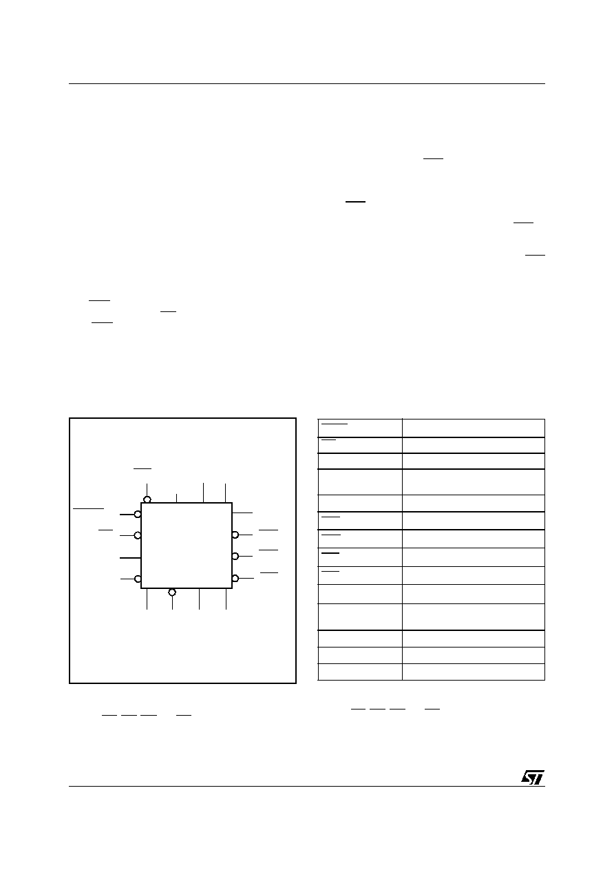
Table 2. Signal Names
Note: See
PIN DESCRIPTIONS
of the full datasheet for details.
1. Normal Mode: Low when V
OUT
is internally switched to
V
CC
and High when V
OUT
is internally switched to battery.
2. SAL, RST, PFO, and BLD are Open Drain.
3. V
REF
only for STM1404A; V
TPU
for STM1404B/C.
AI09682a
V
CC
V
BAT
STM1404
V
SS
V
OUT
V
REF
or
V
TPU
(1)
V
CCSW
(2)
MR
SAL
(3)
BLD
(3)
PFI
TP1 (NH)
TP2
(NL)
TP3
(NH)
TP4
(NL)
PFO
(3)
RST
(3)
Vccsw
(1)
V
CC
Switch Output
MR
Manual (Push-button) Reset Input
PFI
Power-fail Input
TP
1
- TP
4
Independent Physical Tamper
Detect Pins 1 through 4
V
OUT
Supply Voltage Output
RST
(2)
Active-low Reset Output
PFO
(2)
Power-fail Output
SAL
(2)
Security Alarm Output
BLD
(2)
Battery Low Voltage Detect
V
REF
(3)
1.237V Reference Voltage
V
TPU
(3)
Tamper Pull-up
(V
CC
or V
BAT
)
V
BAT
Back-up Supply Voltage
V
CC
Supply Voltage
V
SS
Ground
3/9
STM1404
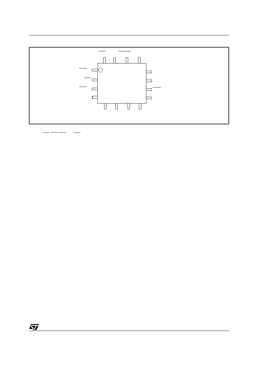
Figure 3. QFN16 Connections
Note: See
PIN DESCRIPTIONS
of the full datasheet for details.
1. Normal Mode: Low when V
OUT
is internally switched to V
CC
and High when V
OUT
is internally switched to battery.
2. SAL, RST, PFO, and BLD are Open Drain.
3. V
REF
only for STM1404A; V
TPU
for STM1404B/C.
1
PFO
(2)
PFI
TP1
(NH)
BLD
(2)
MR
RST
(2)
V
CC
V
CCSW
(1)
V
OUT
V
REF or
V
TPU
(3)
V
BAT
V
SS
AI09683
2
3
4
8
7
6
5
SAL
(2)
9
10
11
12
13
14
15
16
TP2
(NL)
TP3
(NH)
TP4
(NL)
STM1404
4/9
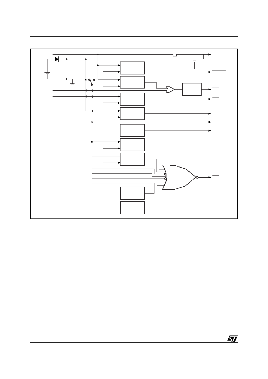
Figure 4. Block Diagram
Note: 1. BAT54J (from STMicroelectronics) recommended.
2. Required for battery-reverse charging protection.
3. Open Drain
4. V
REF
only for STM1404A; V
TPU
for STM1404B/C.
AI09684a
COMPARE @
POWER-UP
VRST
VINT
VOUT
VREF
(4)
1.237V VREF
Generator
COMPARE
COMPARE
COMPARE
COMPARE
COMPARE
High Temp.
Sense
TA > TH
Low Temp.
Sense
TA < TL
trec
Generator
VPFI
VBAT
(1)
VDET
VHV
VLV
VSO
VCC
PFI
TP1 (NH)
TP2 (NL)
TP3 (NH)
TP4 (NL)
MR
RST
(3)
PFO
(3)
BLD
(3)
VCCSW
SAL
(3)
VTPU
(4)
BAT54J
(1,2)

5/9
STM1404
TAMPER DETECTION
Physical
There are four (4) high-impedance physical
tamper detect input pins, 2 normally set to High
(NH) and 2 normally set to Low (NL). Each input is
designed with a glitch immunity. These inputs can
be connected externally to several types of actua-
tor devices (e.g., switches, wire mesh). A tamper
on any one of the four inputs that causes its state
to change will trigger the security alarm (SAL) and
drive it to active-low. Once the tamper condition no
longer exists, the SAL will return to its normal High
state.
TP
1
and TP
3
are set Normally to High (NH). They
are connected externally through a closed switch
or a high-impedance resistor to V
OUT
(in the case
of STM1404A or STM1404A) or V
TPU
(in the case
of STM1404B/C), A tamper condition will be de-
tected when the input pin is pulled low. If not used,
tie the pin to V
OUT
or V
TPU
.
TP
2
and TP
4
are set Normally to Low (NL). They
are connected externally through a high-imped-
ance resistor or a closed switch to V
SS
. A tamper
condition will be detected when the input pin is
pulled high. If not used, tie the pin to V
SS
.
Supply Voltage
The internally switched supply voltage, V
INT
(ei-
ther V
CC
input or V
BAT
input) is continuously mon-
itored. If V
INT
should exceed the over voltage trip
point, V
HV
(set at 4.2V, typical), or should go below
the under voltage trip point, V
LV
(set at 2.0v, typi-
cal). SAL will be driven active-low. Once the
tamper condition no longer exists, the SAL pin will
return to its normal High state.
Temperature
The STM1404 has a built-in, bandgap-based sen-
sor to monitor the temperature. If a preset (cus-
tomer-selectable, factory-programmed) over-
temperature trip point (T
H
) or under-temperature
trip point (T
L
) is exceeded, the SAL is asserted
low.
When no tamper condition exists, SAL is normally
High.
When a tamper is detected, the SAL is activated
(driven low), independent of the part type. V
OUT
can be driven to one of three states, depending on
which variant of STM1404 is being used (see
De-
vice Options, page 1
):
ON;
High-Z; or
Ground (V
SS
).
Note: The STM1404 must be initially powered
above V
RST
to enable the tamper detection
alarms. For example, if the battery is on while V
CC
= 0V, no alarm condition can be detected until V
CC
rises above V
RST
(and t
rec
expires). From this
point on, alarms can be detected either on battery
or V
CC
. This is done to avoid false alarms when
the device goes from no power to its operational
state.