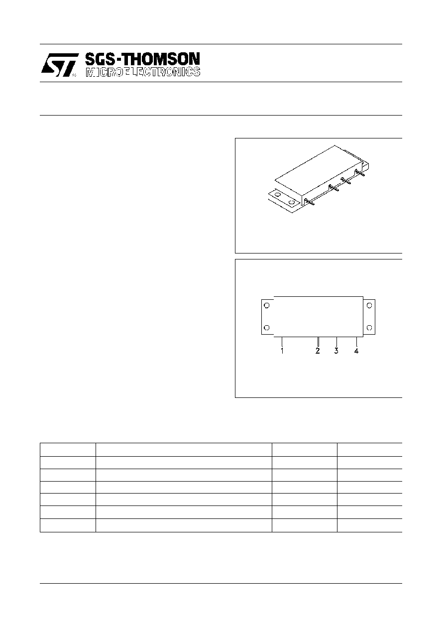
CASE STYLE H150
April 4, 1996
RF POWER MODULES
SATELLITE COMMUNICATIONS APPLICATIONS
.
SATELLITE COMMUNICATIONS
AMPLIFIER
.
1625 - 1665 MHz
.
18/28 VOLTS
.
INPUT/OUTPUT 50 OHMS
.
P
OU T
=
10 W MIN.
.
GAIN
=
30 dB MIN.
DESCRIPTION
The STM1645-10 module is designed for high
power satellite communication applications in
the 1.6 GHz frequency range operating at 28
Volts.
PIN CONNECTION
ABSOLUTE MAXIMUM RATINGS (T
case
=
25
∞
C)
Symbol
Parameter
Value
Un it
V
C 1
DC Supply Voltage
20
Vdc
V
C 2
DC Supply Voltage
32
Vdc
P
IN
RF Input Power
20
mW
P
O UT
RF Output Power
16
W
T
ST G
Sto rage Temperature
-
40 to +100
∞
C
T
C
Operating Case Temperature
-
35 to +70
∞
C
STM1645-10
1. RF Input
2. V
C1
, 18V
3. V
C2
, 28V
4. RF Output
ORDER CODE
STM1645-10
BRANDING
STM1645-10
PRELIMINARY DATA
1/5
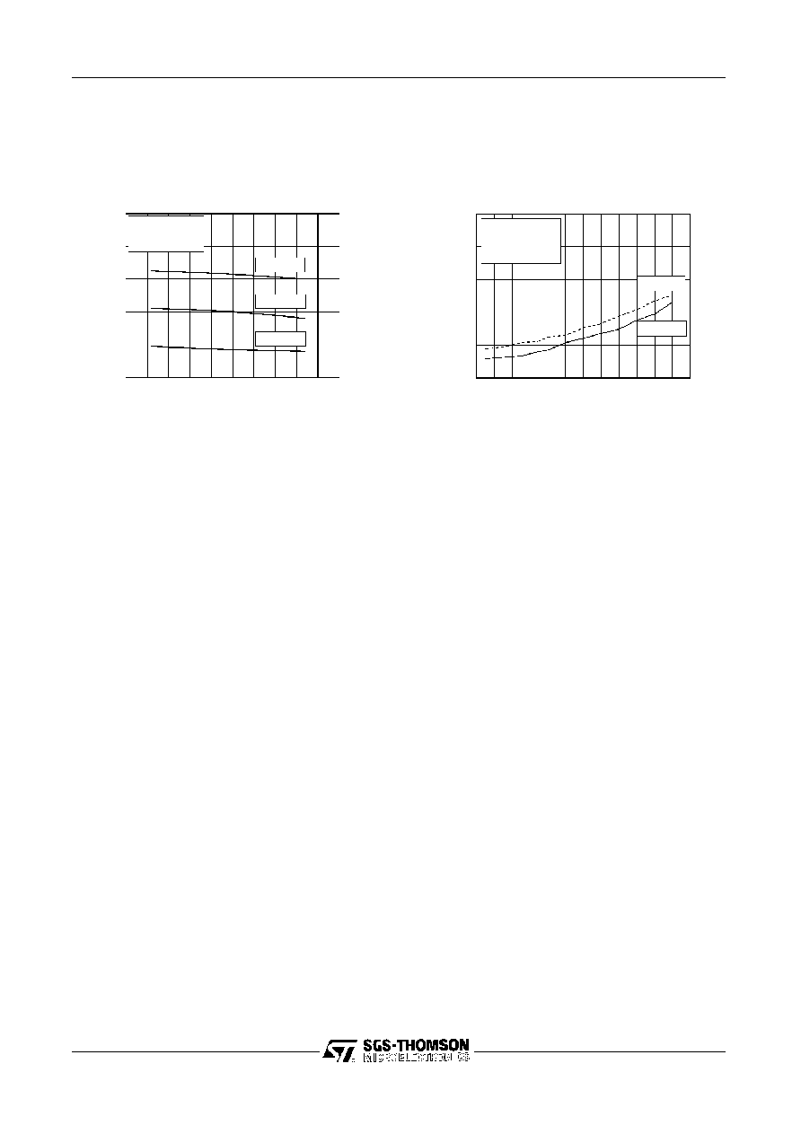
TYPICAL PERFORMANCE
Temperature(Deg C)
Vc2
(Volts)
0
10
20
30
40
50
60
70
80
0
-10
-20
-30
-40
20
22
24
26
28
30
1662 MHz
1626 MHz
Vc1 = 18V
Pin = 10mW
Pout = 10W
VC2 vs FLANGE TEMPERATURE
Frequency (MHz)
Power
Output
(Watts)
1620 1625 1630 1635 1640 1645 1650 1655 1660 1665 1670
10
12
14
16
18
20
Pin = 10mW
Vc1 = 18V
Vc2 = 28V
-35 deg C
+25 deg C
+70 deg C
POWER OUTPUT vs FREQUENCY
STM1645-10
3/5
OPERATION LIMITS
The STM1645-10 power module should never be
operated under any condition which exceeds the
Absolute Maximum Ratings presented on this
data sheet. Nor should the module be operated
continuously at any of the specified maximum rat-
ings. If the module is to be subjected to one or
more of the maximum rating conditions, care must
be taken to monitor other parameters which may
be affected.
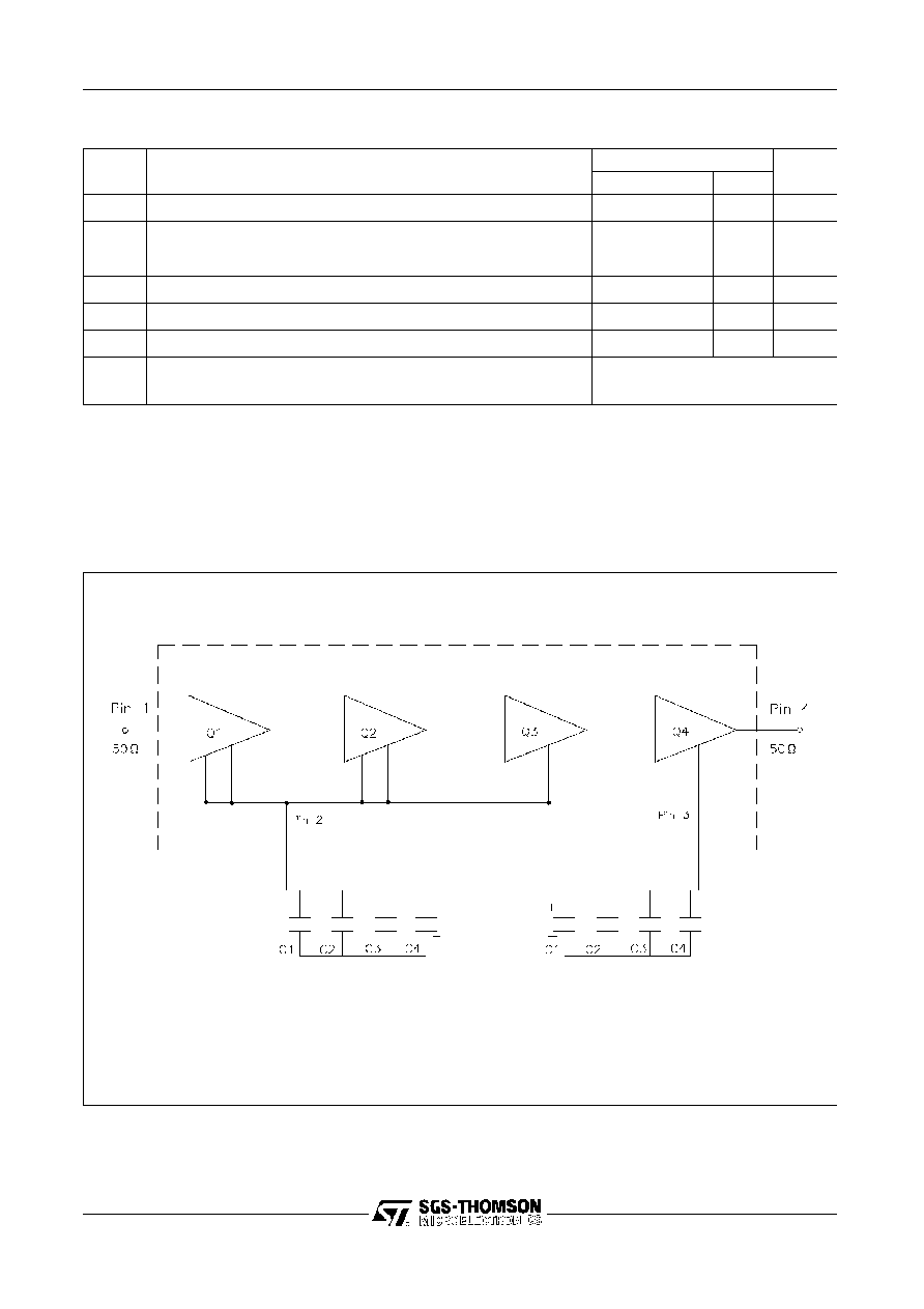
DECOUPLING
Failure to properly decouple any of the voltage
supply pins mayl result in oscillations at certain
operating frequencies. Therefore, it is recom-
mended that these pins be bypassed as indicated
in the Module DC and Test Fixture Configuration
drawing of this data sheet.
POWER CONTROL
The recommeded method of power control for the
STM1645-10 is to set P
IN
= 10mW, V
C1
= 18V
and V
C2
= 28 volts nominal at a flange tempera-
ture of 25
∞
C to achieve an output power of 10
watts. Varing V
C2
will allow stable power control
over a wide range of flange temperature. The cur-
rent consumption of V
C2
is typically 850mA to
900mA for 10 watts power ouput.
MODULE MOUNTING
To insure adequate thermal transfer from the
module to the heatsink, it is recommended that a
satisfactory thermal compound such as Dow
Corning 340, Wakefield 120-2 or equivalent be
applied between the module flange and the
heatsink.
The heatsink mounting surface under the module
should be flat to within
±
0.05mm (
±
0.002 inch).
The module should be mounted to the heatsink
using 3 mm (or 4-40) or equivalent screws tor-
qued to 5-6 kg-cm (4-6 in-lb).
The module leads should be attached to equip-
ment PC board using 180
∞
C solder applied to the
leads with a properly grounded soldering iron tip,
not to exceed 195
∞
C, applied a minimum of 2mm
(0.080 inch) from the body of the module for a
duration not to exceed 15 seconds per lead. It is
imperative that no other portion of the module,
other than the leads, be subjected to tempera-
tures in excess of 100
∞
C (maximum storage tem-
perature), for any period of time, as the plastic
moulded cover, internal components and sealing
adhesives may be adversely affected by such
conditions.
Due to the construction techniques and materials
used within the module, reflow soldering of the
flange heatsink or leads, is not recommended.
APPLICATIONS RECOMMENDATIONS
STM1645-10
4/5
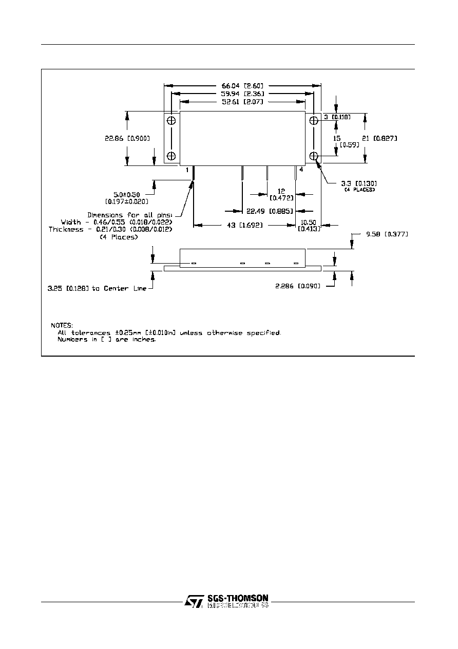
Ref.: Dwg. No. 1018019 rev. D
PACKAGE MECHANICAL DATA
Inform ati on furni shed is believed to be accurate and reliable. However, SGS-THOMSON Microelectronics assumes no responsibili ty for
the consequences of use of such information nor for any infringement of patents or other rights of thir d parties w hic h may result from
its use. No lic ense is granted by impli cation or otherwise under any patent or patent rights of SGS-THOMSON Mi croele ctr oni cs.
Specificati ons mentioned i n this publication are subj ect to change without notice. T hi s publication supersedes and repl aces all
information pr evio usly supplied. SGS-T HOMSON Mi croelectronics products are not authorized for use as critical components in life
support devices or systems without express written approval of SGS-THOMSON Mi croelectronics.
©
1996 SGS -T HOMSON Microelectronics - All Rights Reserved
SGS-THOMSON Microelectronics GROUP O F COMPANIES
Australia - B razi l - France - Germany - Hong Kong - Ital y - Japan - Korea - Malaysia -
Mal ta - Mor occo - The Netherlands - S ingapore - Spain - Sweden - Switzerland - Taiw an -
T hai land - Uni ted Kingdom - U.S.A.
STM1645-10
5/5