 | –≠–ª–µ–∫—Ç—Ä–æ–Ω–Ω—ã–π –∫–æ–º–ø–æ–Ω–µ–Ω—Ç: STM901-30 | –°–∫–∞—á–∞—Ç—å:  PDF PDF  ZIP ZIP |
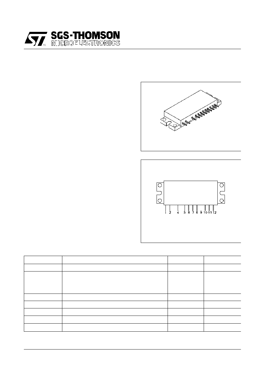
CASE STYLEH141
RF POWER MODULE
LINEAR BASE STATION APPLICATIONS
.
LINEAR POWER AMPL IFIER
.
860 - 900 MHz
.
26 VOLTS
.
INPUT/OUTPUT 50 OHMS
.
P
OU T
=
+44.7 dBm PEP
.
GAIN
=
35 dB MIN.
DESCRIPTION
The STM901-30 module is designed for digital
cellular radio base station applications in the
860-900 MHz frequency range operating at
26V.
The STM901-30 is designed to meet the low
distortion, high linearity requirements of mod-
ern digital cellular base station equipment.
PIN CONNECTION
ABSOLUTE MAXIMUM RATINGS (Tcase
=
25
∞
C)
STM901-30
1. RF Input
2.
V
G1
3.
deleted 4. V
G2
5. V
D
6.
V
B1
7.
Cap
1
8. V
C1
9. V
B2
10. Cap
2
11. V
C2
12. RF Output
ORDER CODE
STM901-30
BRANDING
STM901-30
Symbol
Parameter
Value
Uni t
V, V
D
, V
C1
, V
C2
DC Supply Voltage
28
Vdc
I
Q 1
Bias Current @ V
=
26V, 1st Stage
0.40
Adc
I
Q 2
Bias Current @ V
=
26V, 2nd Stage
0.40
Adc
I
Q 3
Bias Current @ V
=
26V, 3rd Stage
0.54
Adc
I
Q 4
Bias Current @ V
=
26V, 4th Stage
1.62
Adc
P
I N
RF Input Power
(P
OUT
< 44.7 dBm PEP)
14
dBm PEP
P
OU T
RF Output Power
(V
=
26V)
48
dBm PEP
T
STG
Storage Temperature
-
30 to +100
∞
C
T
O PE R
Operating Temperature
-
30 to +100
∞
C
October 31, 1997
1/8
ELECTRICAL SPECIFICATIONS (T
case
= 25
∞
C, V
D
, V
C1
, V
C2
= 26V) (I
DQ 1
= 100mA,
I
DQ 2
= 180mA, I
CQ 1
= 50mA, I
C Q2
=150mA)
Symbol
Parameter
T est Cond iti ons
Value
Un it
Min.
Typ.
Max.
BW
Frequency Range
860
--
900
MHz
G
P
Power Gain
P
OUT
=
+44.7 dBm PEP
35
38
--
dB
dt
*
Double-Tone
Efficiency
P
OUT
=
+44.7 dBm PEP
27
30
--
%
Input VSWR
P
OUT
=
+44.7 dBm PEP
--
1.5:1
3:1
IMD*
Intermodulation
Distortion
P
OUT
=
+44.7 dBm PEP
--
-
33
-
26
dBT**
--
Load Mismatch
VSWR
=
5:1
V
=
26Vdc
P
OUT
=
+44.7 dBm PEP
No Degradation in Output
Power
Note:
* Two- Tone test; 20 KHz separation
** dBT - i n dB, refer enced to tone level (See Figure 1 below)
20 kHz
PEP (Peak Envelope Power) Carrier Level
Total Avg. Power of Two Tone
AVERAGE Power of Ea ch Tone
3 dB min
3 dB min
26 dB min
freq
Max IMD in dBT
Figure 1
STM901-30
2/8
October 31, 1997
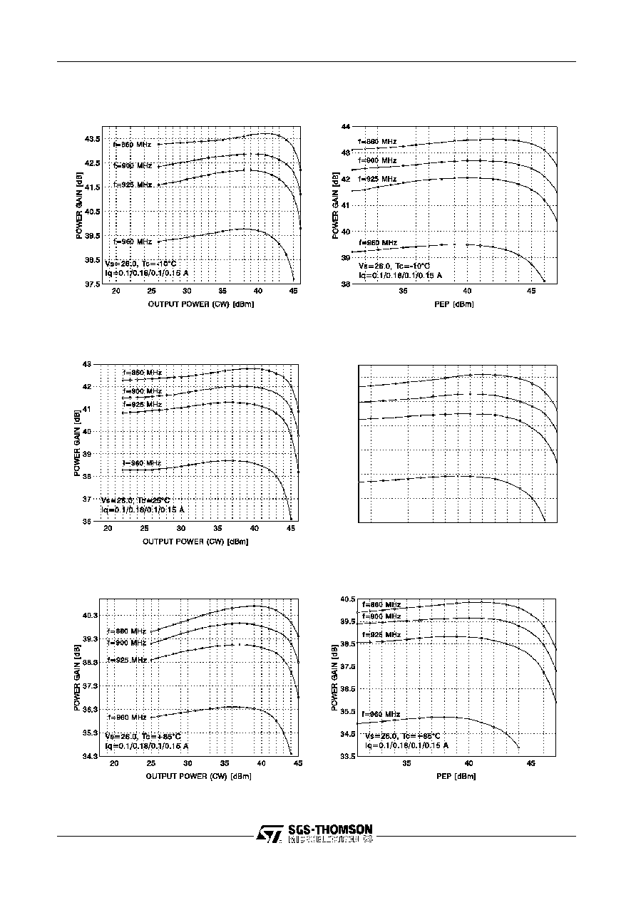
POWER GAIN vs OUTPUT POWER &
FREQUENCY
POWER GAIN vs OUTPUT POWER &
FREQUENCY
POWER GAIN vs OUTPUT POWER &
FREQUENCY
POWER GAIN vs PEP & FREQUENCY
POWER GAIN vs PEP & FREQUENCY
POWER GAIN vs PEP & FREQUENCY
PEP [dBm]
POWER
GAIN
[dB]
35
40
45
36.5
37.5
38.5
39.5
40.5
41.5
42.5
f=900 MHz
f=860 MHz
f=925 MHz
f=960 MHz
Vs=26.0, Tc=25
∞
C
Iq=0.1/0.18/0.1/0.15 A
TYPICAL PERFORMANCE
STM901-30
October 31, 1997
3/8
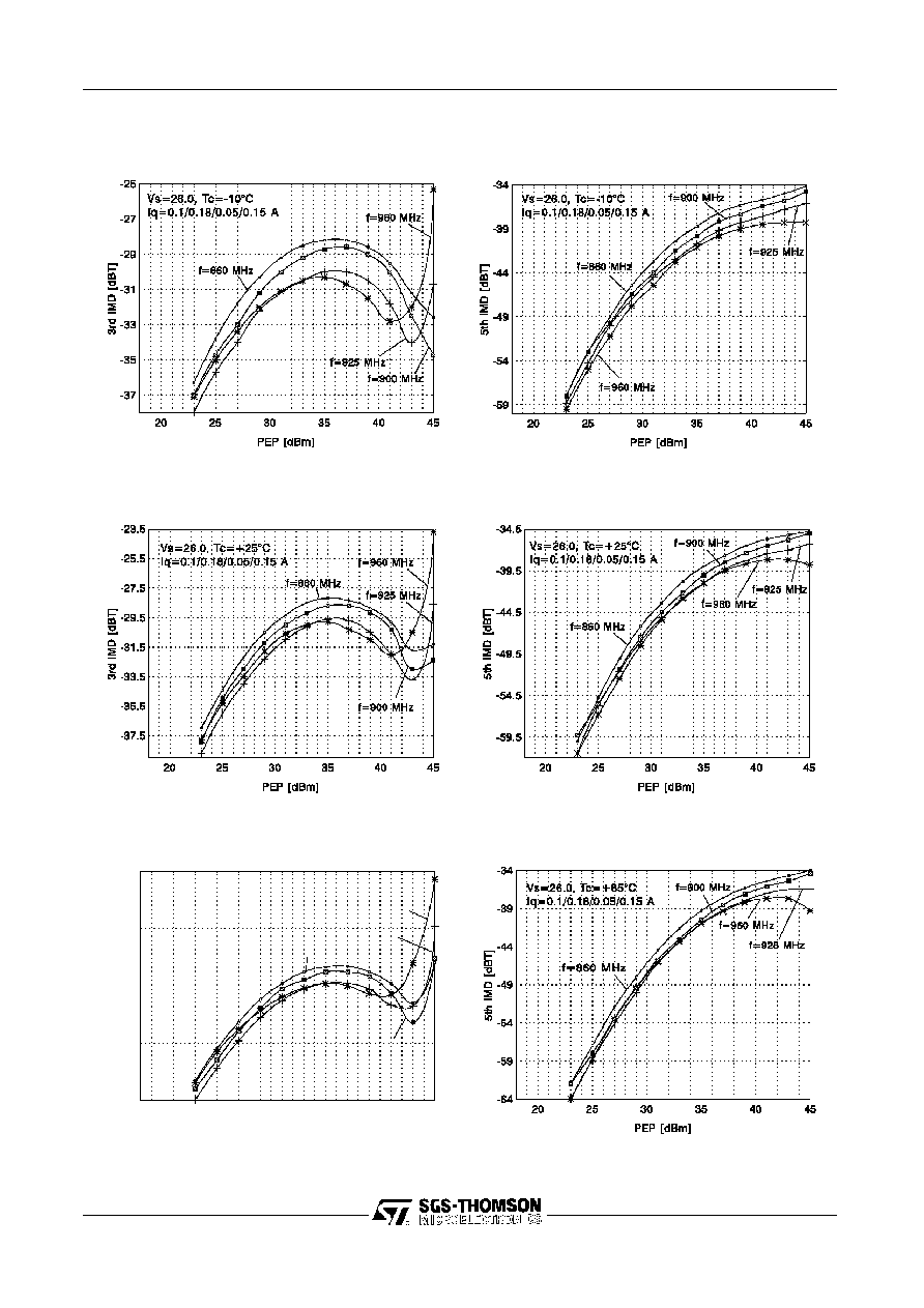
5th ORDER IMD vs PEP
5th ORDER IMD vs PEP
5th ORDER IMD vs PEP
3rd ORDER IMD vs PEP
3rd ORDER IMD vs PEP
3rd ORDER IMD vs PEP
PEP [dBm ]
3rd
IMD
[dBT]
20
25
30
35
40
45
-20
-25
-30
-35
-40
f=900 MHz
f=860 MHz
f=925 M Hz
f=960 MHz
V s=26.0, Tc=+85
∞
C
I q=0.1/0.18/0.05/0.15 A
TYPICAL PERFORMANCE
STM901-30
4/8
October 31, 1997
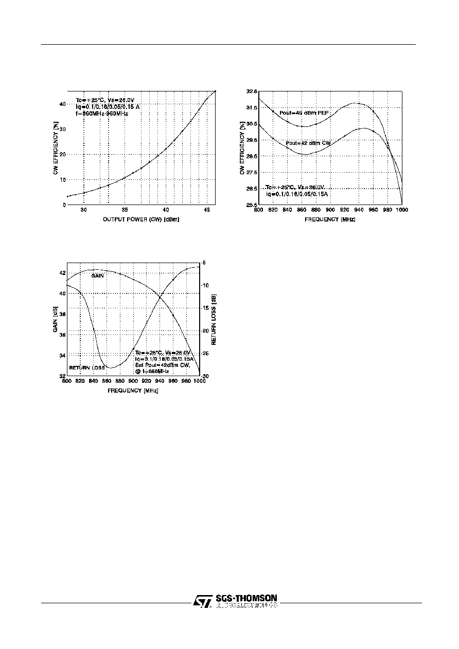
GAIN & RETURN LOSS vs FREQUENCY
EFFICIENCY vs FREQUENCY
CW EFFICIENCY vs OUTPUT POWER
& FREQUENCY
TYPICAL PERFORMANCE
STM901-30
October 31, 1997
5/8
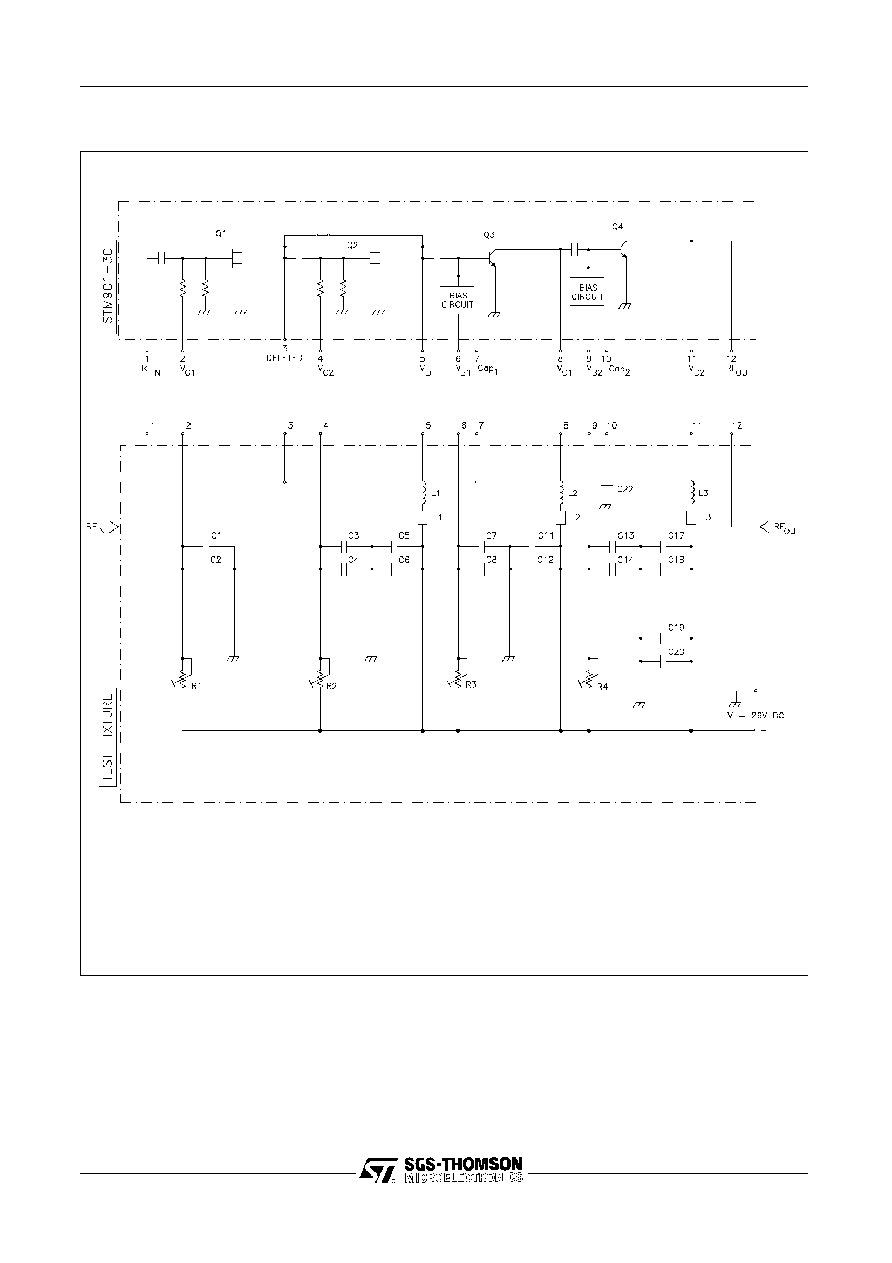
C1, C3, C5, C7, C11, C13, C 17
: 100 pF
C2, C4, C6, C8, C12, C14, C 18
: .001
µ
F
C19 : .1
µ
F
C20, C22 : 100
µ
F
F1, F2, F3
: FAIR-RITE #2664000101
L1, L2, L3
: 5 Turns of 24 AWG Wi re, Inner Dia meter
1.27mm
R1, R2, R3, R4 : 20 KOHM
Setting Bias: (Ex.: IQ1
=
.1A, IQ2
=
.18A, IQ3
=
.050A, IQ4
=
.150A)
1.
Set all variable resistors clockwise. (No bias current flows through
transistors when all variable resistors are set clockwise.)
2.
Record stationary current IO.
3.
Adjust R1 for (IO + 100)mA.
4.
Adjust R2 for (IO + 100 + 180)mA.
5.
Adjust R3 for (IO + 100 + 180 + 50)mA.
6.
Adjust R4 for (IO + 100 + 180 + 50 + 150)mA.
MODULE DC AND TEST FIXTURE CONFIGURATION
STM901-30
6/8
October 31, 1997

APPLICATIONS RECOMMENDATIONS
OPERATION LIMITS
The STM901-30 power module should never be op-
erated under any condition which exceeds the Ab-
solute Maximum Ratings presented on this data
sheet. Nor should the module be operated continu-
ously at any of the specified maximum ratings. If
the module is to be operated under any condition
such that it may be subjected to one or more of the
maximum rating conditions, care must be taken to
monitor other parameters which may be affected.
DECOUPLING
Failure to properly decouple any of the voltage sup-
ply pins will result in oscillations at certain operating
frequencies. Therefore, it is recommended that
these pins be bypassed as indicated in the Module
DC and Test Fixture Configuration drawing of this
data sheet.
MODULE MOUNTING
To insure adequate thermal transfer from the mod-
ule to the heatsink, it is recommended that a satis-
factory thermal compound such as Dow Corning
340, Wakefield 120-2 or equivalent be applied be-
tween the module flange and the heatsink.
The heatsink mounting surface under the module
should be flat to within +/- 0.05 mm (+/- 0.002
inch). The module should be mounted to the
heatsink using 3 mm (or 4-40) or equivalent screws
torqued to 5-6 kg-cm (4-6 in-lb).
The module leads are attached to the equipment
PC board using 180
∞
C solder applied to the leads
with a properly grounded soldering iron tip, not to
exceed 195
∞
C, applied a minimum of 2 mm (0.080
inch) from the body of the module for a duration not
to exceed 15 seconds per lead. It is imperative that
no other portion of the module, other than the
leads, be subjected to temperatures in excess of
100
∞
C (maximum storage temperature), for any pe-
riod of time, as the plastic moulded cover, internal
components and sealing adhesives may be ad-
versely affected by such conditions.
Due to the construction techniques and the materi-
als used within the module, reflow soldering of the
flange heatsink or the leads, is not recommended.
THERMAL CONSIDERATIONS
It will be necessary to provide a suitable heatsink in
order to maintain the module flange temperature at
or below the maximum case operating temperature.
In a case where the module output power will be
limited to +44.7 dBm (30W PEP) and designing for
the worst case double-tone efficiency of 25%, the
power dissipated by the module will be 48 watts.
The heatsink must be designed such that the ther-
mal rise will be less than the difference between
the maximum ambient temperature at which the
module will operate and the maximum operating
case temperature of the module while dissipating
48 watts.
At T
case
=
+85
∞
C, V
=
26v, I
Q1
=
0.1A, I
Q2
=
0.18A,
I
Q3
=
0.05A, I
Q4
=
0.2A, Z
L
=
50 ohms and P
OUT
=
+44.7dBm PEP, maximum junction temperatures for
the individual transistors should be below the fol-
lowing values:
Q1 = 115
∞
C
Q2 = 130
∞
C
Q3 = 125
∞
C
Q4 = 145
∞
C
STM901-30
October 31, 1997
7/8
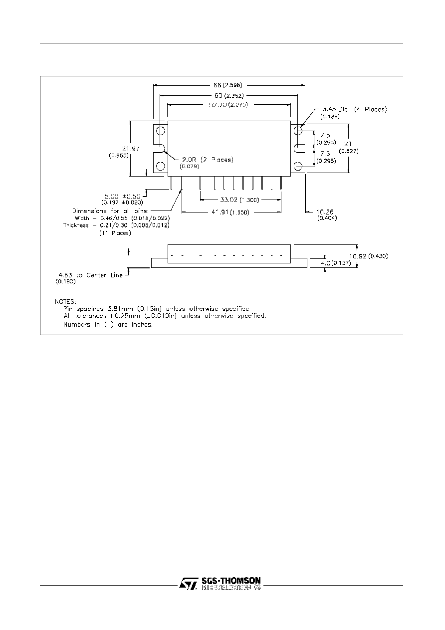
PACKAGE MECHANICAL DATA
UDCS No. 1010946 rev D
Inform ati on furni shed is believed to be accurate and reliable. However, SGS-THOMSON Microelectronics assumes no responsibili ty for
the consequences of use of such information nor for any infringement of patents or other rights of thir d parties w hic h may result from
its use. No lic ense is granted by impli cation or otherwise under any patent or patent rights of SGS-THOMSON Mi croele ctr oni cs.
Specificati ons mentioned i n this publication are subj ect to change without notice. T hi s publication supersedes and repl aces all
information pr evio usly supplied. SGS-T HOMSON Mi croelectronics products are not authorized for use as critical components in life
support devices or systems without express written approval of SGS-THOMSON Mi croelectronics.
©
1997 SGS -T HOMSON Microelectronics - All Rights Reserved
SGS-THOMSON Microelectronics GROUP O F COMPANIES
Austral ia - Br azil - Canada - China - F rance - Germany - Italy - Japan - Korea
Mal aysia - Malta - Morocco - Th e Netherl ands - Singapor e - Spain - Sweden - Switzerla nd
Taiwan - Thailand - United Kingdom - U.S.A.
RF Products Division
141 Commerce Drive Montgomeryville, PA 18936
tel 215-361-6400 fax 215-362-1293
STM901-30
8/8
October 31, 1997