
September 2005
1/21
21
Rev. 1
STMAV340
Low ON Resistance Quad, SPDT, Wide-Bandwidth Video Switch
Features
Bi-directional operation
4 input/output channels analog video switch
Wide bandwidth 300MHz
Low 4
switch resistance between two ports
Excellent R
ON
matching between channels
Minimal propagation delay through the switch
Low quiescent current consumption
V
CC
Operating Range: 4.0V to 5.5V
Zero bounce in flow-through mode
Control inputs compatible with TTL level
All input/output pins are on the same side
facilitates PCB routing
Data and control inputs provide the
undershoot clamp diode
Guaranteed break-before-make timing
High ESD rating: > 2kV HBM
40°C to 85°C operating temperature range
Suitable for both RGB and Composite-Video
Switching
Available in a small TSSOP16 package
Applications
Advanced TVs
Front projectors
LCD Monitors
Notebook PCs
DVD Players
Order Codes
Description
The STMAV340 is a bidirectional quad (4
channel), high speed single pole/double throw
(SPDT), low power CMOS TTL-compatible analog
video switch designed for advanced video
applications which demand superior image
quality. The low ON Resistance (R
ON
) of the
switch allows inputs to be connected to outputs
without adding propagation delay or generating
additional ground bounce noise.
STMAV340 is designed for very low cross-talk,
low bit-to-bit skew, high channel-to-channel noise
isolation, and low I/O capacitance. The switch
offers very little or practically no attenuation of the
high speed signals at the outputs, thus preserving
the signal integrity enough to pass stringent
requirements.
The STMAV340 is able to simplify the PCB routing
on inputs and outputs as well as reduce the
overall BOM costs by eliminating the need for
more costly input-output controllers.
TSSOP16
www.st.com
Part Number
Temperature Range
Package
Comments
STMAV340
40
°
C to +85
°
C
TSSOP16
STMAV340TTR

STMAV340
2/21
Contents
1
Summary Description . . . . . . . . . . . . . . . . . . . . . . . . . . . . . . . . . . . . . . . . . . 3
1.1
Functional Description . . . . . . . . . . . . . . . . . . . . . . . . . . . . . . . . . . . . . . . . . . 3
2
Pin Configuration . . . . . . . . . . . . . . . . . . . . . . . . . . . . . . . . . . . . . . . . . . . . . 4
3
Application Diagrams . . . . . . . . . . . . . . . . . . . . . . . . . . . . . . . . . . . . . . . . . . 5
3.1
Power Supply Sequencing . . . . . . . . . . . . . . . . . . . . . . . . . . . . . . . . . . . . . . . 5
4
Maximum Ratings . . . . . . . . . . . . . . . . . . . . . . . . . . . . . . . . . . . . . . . . . . . . . 6
5
Electrical Characteristics . . . . . . . . . . . . . . . . . . . . . . . . . . . . . . . . . . . . . . . 7
6
Test Circuit and Diagrams . . . . . . . . . . . . . . . . . . . . . . . . . . . . . . . . . . . . . . 9
7
Package Mechanical Data . . . . . . . . . . . . . . . . . . . . . . . . . . . . . . . . . . . . . . 18
8
Revision History . . . . . . . . . . . . . . . . . . . . . . . . . . . . . . . . . . . . . . . . . . . . . 20
STMAV340
1 Summary Description
3/21
1 Summary
Description
1.1 Functional
Description
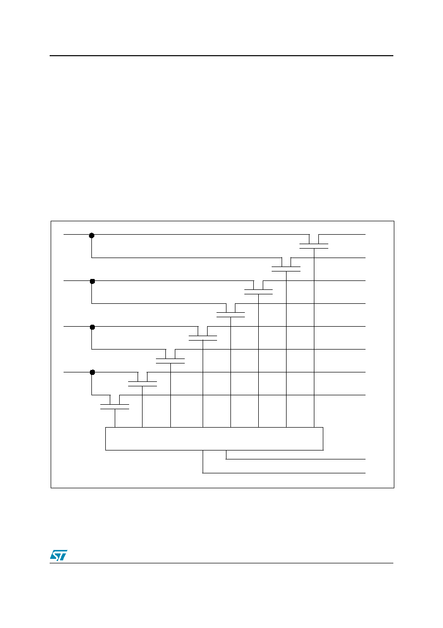
The STMAV340 is a high bandwidth, analog video switch. It is low ON-resistance and low I/O
capacitance result in a very small propagation delay.
When OE_N is set to LOW, the select (S) pin connects port A to the selected port B or port C
output. When OE_N is set to HIGH, the switch is OPEN and a high-impedance state exists
between the A port and B/C ports.
Low differential gain and phase make this switch ideal for component and RGB video
applications. This device has high bandwith and low crosstalk, making it ideal for high
frequency applications as well.
Figure 1.
Functional Diagram
Flow Cont rol
1A
2A
3A
4A
1B
1C
2B
2C
3B
3C
4B
4C
OE_N
S
Flow Cont rol
1A
2A
3A
4A
1B
1C
2B
2C
3B
3C
4B
4C
OE_N
S
2 Pin Configuration
STMAV340
4/21
2 Pin
Configuration
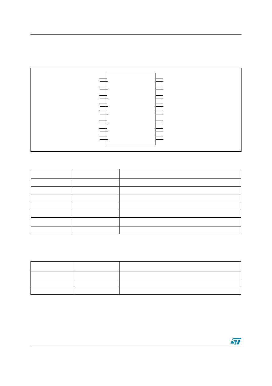
Table 1.
Pin Description
Note: 1 Tie to V
CC
through a pull-up resistor. The minimum value of the resistor is determined by the
current-sinking capability of the driver.
Table 2.
Truth Table
Figure 2.
Pin Configuration (Top View )
Symbol
Type
Name and Functions
OE_N
IN
Bus Switch Enable
Note: 1
S
IN
Select Input
1A ,2A ,3A ,4A
IN/OUT
Port A; Analog Video I/Os
1B ,2B ,3B ,4B
IN/OUT
Bus B; Analog Video I/Os
1C, 2C, 3C, 4C
IN/OUT
Bus C; Analog Video I/Os
V
CC
Power supply
GND
Ground
OE_N
S
ON Switch
0
0
1B,2B,3B,4B
0
1
1C,2C,3C,4C
1
X
Disabled
1B
1C
2B
2C
3B
3C
4B
4C
V
CC
OE_N
S
1A
2A
3A
4A
GND
1
2
3
4
5
6
7
8
9
10
11
12
13
14
15
16
1B
1C
2B
2C
3B
3C
4B
4C
V
CC
OE_N
S
1A
2A
3A
4A
GND
1
2
3
4
5
6
7
8
9
10
11
12
13
14
15
16
STMAV340
3 Application Diagrams
5/21
3 Application
Diagrams
3.1 Power
Supply
Sequencing
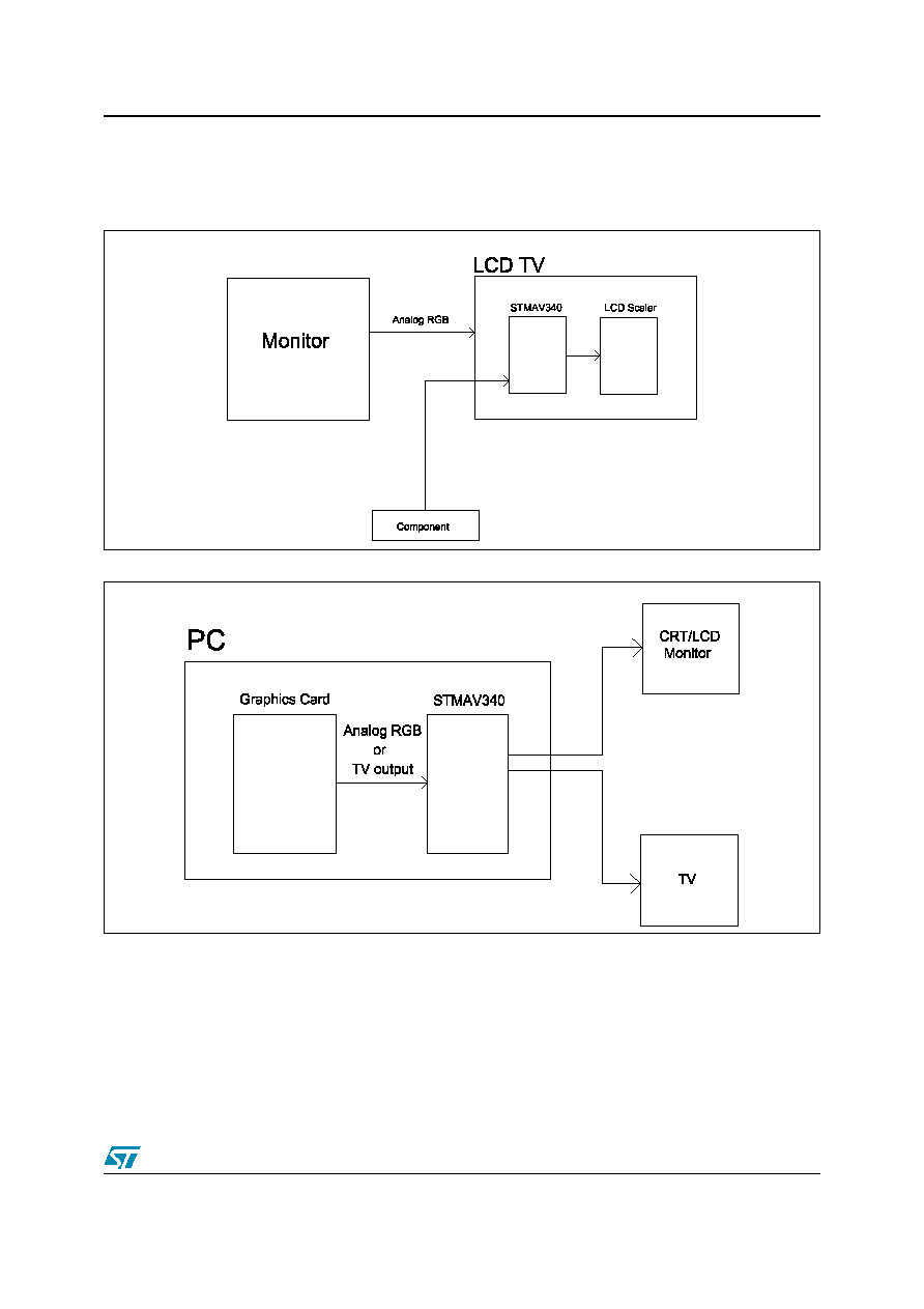
Proper power-supply sequencing is advised for all CMOS devices. Applying V
CC
before
sending any signals to the input/output or control pins is recommended.
Figure 3.
STMAV340 2-to-1 Analog Video Switch Used in an LCD TV
Figure 4.
STMAV340 1-to-2 Analog Video Switch Used in a PC