Äîêóìåíòàöèÿ è îïèñàíèÿ www.docs.chipfind.ru
1/9
May 2005
I
LOW R
ON
: 5.5
TYPICAL
I
V
CC
OPERATING RANGE: 3.0 TO 3.6 V
I
LOW CURRENT CONSUMPTION: 20 µA
I
ESD HBM MODEL: > 2 KV
I
CHANNEL ON CAPACITANCE: 7.5 pF
TYPICAL
I
SWITCHING TIME SPEED: 9 ns
I
NEAR TO ZERO PROPAGATION DELAY:
250 ps
I
VERY LOW CROSS TALK: -40 dB AT
250MHz
I
BIT TO BIT SKEW: 200 ps
I
> 450 MHZ -3db TYPICAL BANDWIDTH
I
THREE SWITCH S.P.D.T FOR LED
SUPPORTING
I
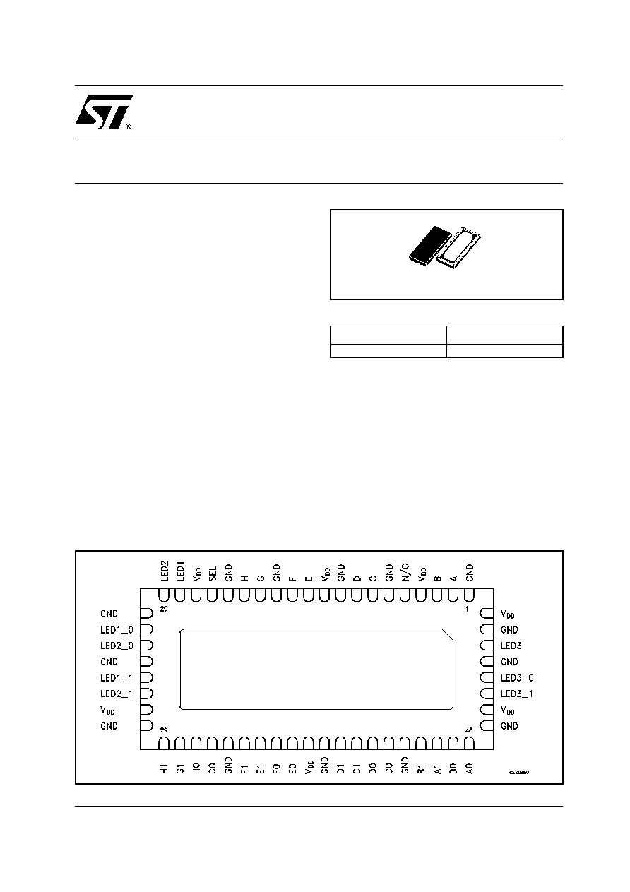
PACKAGE: QFN56
I
Pb FREE
DESCRIPTION
The STMUX1000L is a 16 to 8 Bit multiplexer/
demultiplexer low R
ON
bidirectional LAN Switch
designed for various standard, such as 10/100/
1000 Ethernet.
It is designed for very low Cross Talk, low bit to bit
skew and low I/O capacitance.
The differential signal from the Gigabit Ethernet
Transceiver is multiplexed in one of two selected
output while the unselected switch go to Hi-Z
status.
The device integrates three 16
switches,
S.P.D.T. (Single Pole Dual Throw Channel), for
LED supporting.
STMUX1000L
GIGABIT LAN ANALOG SWITCH
16-BIT TO 8-BIT MULTIPLEXER
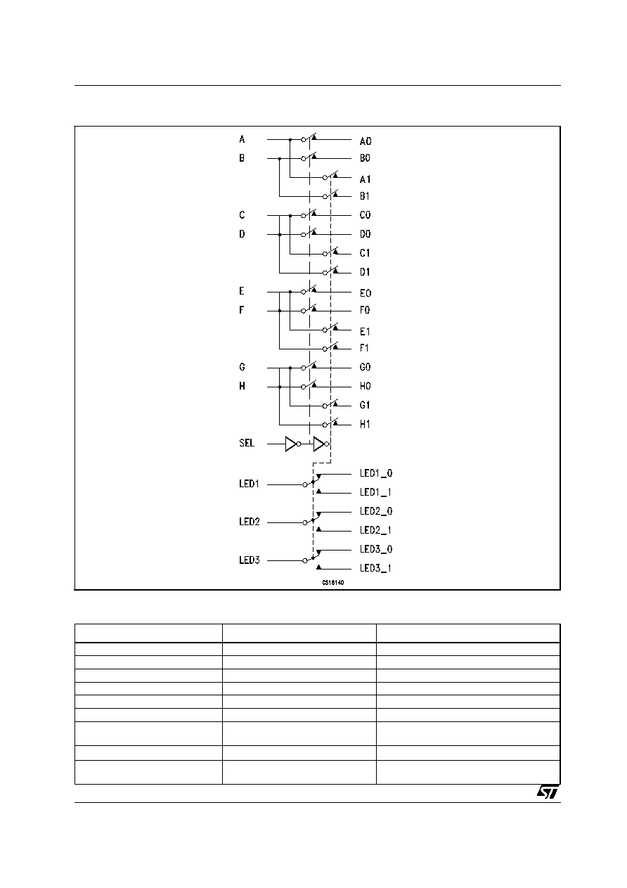
Figure 1: Pin Connection (Top Through View)
Table 1: Order Codes
PACKAGE
T & R
QFN
STMUX1000LQTR
QFN56
Rev. 2
STMUX1000L
2/9
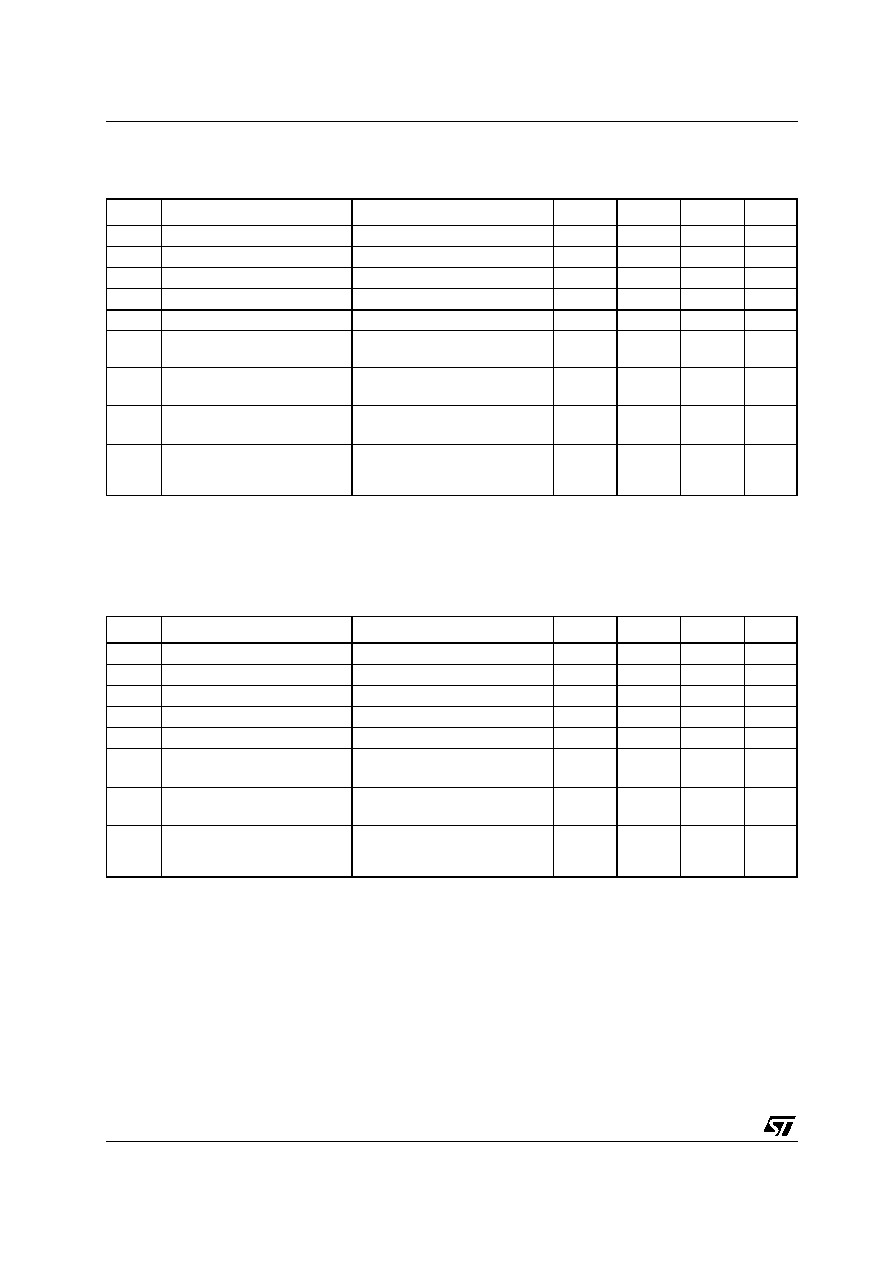
Figure 2: Input Equivalent Circuit
Table 2: Pin Description
PIN N°
SYMBOL
NAME AND FUNCTION
2, 3, 7, 8, 11, 12, 14, 15
A, B, C, D, E, F, G, H
8 Bit Bus
48, 47, 43, 42, 37, 36, 32, 31
A0, B0, C0, D0, E0, F0, G0, H0
8 Bit Multiplexed to Bus 0
46, 45, 41, 40, 35, 34, 30, 29
A1, B1, C1, D1, E1, F1, G1, H1
8 Bit Multiplexed to Bus 1
5
N/C
Not Connected
17
SEL
BUS and LED Switch Selection
19, 20, 54
LED1, LED2, LED3
LED Switch Input
22, 23, 25, 26, 51, 52
LED1_0, LED2_0, LED1_1,
LED2_1, LED3_0, LED3_1
LED Switch Output
4, 10, 18, 27, 38, 50, 56
V
DD
Supply Voltage
1, 6, 9, 13, 16, 21, 24, 28,
33, 39, 44, 49, 53, 55
GND
Ground

STMUX1000L
3/9
Table 3: Lan Switch Function Table
Table 4: Led Switch Function Table
Table 5: Absolute Maximum Ratings
Absolute Maximum Ratings are those values beyond which damage to the device may occur. Functional operation under these conditions is
not implied.
(*) If not exceed the max limit of P
D
.
Table 6: DC Electrical Characteristics For Gigabit Ethernet LAN8/16MUX/DEMUX
(T
A
= -40 to 85°C, V
CC
= 3.3V ±10%)
Note 1: Measured by voltage drop between Channels @ indicated current trough the switch. On-Resistance is determinate by the lower the
voltage on the two.
Note 2: Flatness is defined as the difference the R
ONMAX
and R
ONMIN
of On-Resistance over the specified range condition.
Note 3:
R
ON
measured @ same V
CC
, temperature and voltage level.
SE
FUNCTION
L
8 Bit Bus to 8 Bit Multiplexed Bus 0
H
8 Bit Bus to 8 Bit Multiplexed Bus 1
SE
FUNCTION
L
Led Switch Input connected to Led Switch Output X_0
H
Led Switch Input connected to Led Switch Output X_1
Symbol
Parameter
Value
Unit
V
CC
Supply Voltage to Ground
-0.5 to 4
V
V
I
DC Input Voltage
-0.5 to 4
V
V
IC
DC Control Input Voltage
-0.5 to 4
V
I
O
DC Output Current (*)
120
mA
P
D
Power Dissipation
0.5
W
T
stg
Storage Temperature
-65 to 150
°C
T
L
Lead Temperature (10 sec)
300
°C
Symbol
Parameter
Test Conditions
Min.
Typ.
Max.
Unit
V
IH
Voltage Input High
High Level Guaranteed
2
V
V
IL
Voltage Input Low
Low Level Guaranteed
-0.5
0.8
V
V
IK
Clamp Diode Voltage
V
CC
= 3.6V, I
IN
= -18mA
-0.8
-1.2
V
I
IH
Input High Current
V
CC
= 3.6V, V
IN
= V
CC
±
5
µ
A
I
IL
Input Low Current
V
CC
= 3.6V, V
IN
= GND
±
5
µ
A
I
OFF
Power Down Leakage Current
V
CC
= 0V, A to H V = 0V,
A0 to H0 and A1 to H1
3.6V
±
5
µ
A
R
ON
Switch ON Resistance (1)
V
CC
= 3.0 V, V
IN
= 1.5 to V
CC
I
IN
= -40mA
5.5
7.5
R
FLAT
ON Resistance FLATNESS
(1, 2)
V
CC
= 3.0 V, V
IN
@ 1.5 and V
CC
I
IN
= -40mA
0.8
R
ON
ON Resistance Match between
channel
R
ON
= R
ONMAX
-R
ONMIN
(1,3)
V
CC
= 3.0 V, V
IN
= 1.5 to V
CC
I
IN
= -40mA
0.5
1
STMUX1000L
4/9
Table 7: DC Electrical Characteristics For 10/100 Ethernet LAN8/16MUX/DEMUX
(T
A
= -40 to 85°C, V
CC
= 3.3V ±10%)
Note 1: Measured by voltage drop between Channels @ indicated current trough the switch. On-Resistance is determinate by the lower the
voltage on the two.
Note 2: Flatness is defined as the difference the R
ONMAX
and R
ONMIN
of On-Resistance over the specified range condition.
Note 3:
R
ON
measured @ same V
CC
, temperature and voltage level.
Table 8: Led Switches DC Electrical Characteristics
(T
A
= -40 to 85°C, V
CC
= 3.3V ±10%)
Note 1: Measured by voltage drop between Channels @ indicated current trough the switch. On-Resistance is determinate by the lower the
voltage on the two.
Note 2: Flatness is defined as the difference the R
ONMAX
and R
ONMIN
of On-Resistance over the specified range condition.
Note 3:
R
ON
measured @ same V
CC
, temperature and voltage level.
Symbol
Parameter
Test Conditions
Min.
Typ.
Max.
Unit
V
IH
Voltage Input High
High Level Guaranteed
2
V
V
IL
Voltage Input Low
Low Level Guaranteed
-0.5
0.8
V
V
IK
Clamp Diode Voltage
V
CC
= 3.6V, I
IN
= -18mA
-0.7
-1.2
V
I
IH
Input High Current
V
CC
= 3.6V, V
IN
= V
CC
±
5
µ
A
I
IL
Input Low Current
V
CC
= 3.6V, V
IN
= GND
±
5
µ
A
I
OFF
Power Down Leakage Current
V
CC
= 0V, A to H V = 0V,
A0 to H0 and A1 to H1
3.6V
±
5
µ
A
R
ON
Switch ON Resistance (1)
V
CC
= 3.0 V, V
IN
= 1.25 to V
CC
I
IN
= -40mA
5.5
7.5
R
FLAT
ON Resistance FLATNESS
(1, 2)
V
CC
= 3.0 V, V
IN
@ 1.25 and V
CC
I
IN
= -40mA
0.9
R
ON
ON Resistance Match between
channel
R
ON
= R
ONMAX
-R
ONMIN
(1, 3)
V
CC
= 3.0 V, V
IN
= 1.25 to V
CC
I
IN
= -40mA
0.5
1
Symbol
Parameter
Test Conditions
Min.
Typ.
Max.
Unit
V
IH
Voltage Input High
High Level Guaranteed
2
V
V
IL
Voltage Input Low
Low Level Guaranteed
-0.5
0.8
V
V
IK
Clamp Diode Voltage
V
CC
= 3.6V, I
IN
= -18mA
-0.7
-1.2
V
I
IH
Input High Current
V
CC
= 3.6V, V
IN
= V
CC
±
5
µ
A
I
IL
Input Low Current
V
CC
= 3.6V, V
IN
= GND
±
5
µ
A
R
ON
Switch ON Resistance (1)
V
CC
= 3.0 V, V
IN
= 1.25 to V
CC
I
IN
= -40mA
16
25
R
FLAT
ON Resistance FLATNESS
(1, 2)
V
CC
= 3.0 V, V
IN
@ 1.25 and V
CC
I
IN
= -40mA
8
R
ON
ON Resistance Match between
channel
R
ON
= R
ONMAX
-R
ONMIN
(1, 3)
V
CC
= 3.0 V, V
IN
= 1.25 to V
CC
I
IN
= -40mA
1
2
STMUX1000L
5/9
Table 9: Capacitance Lan 8/16 MUX/DEMUX (T
A
= 25°C, f = 1 MHz)
Note 4: x = A to H, x0 = A0 to H0, x1 = A1 to H1.
Table 10: Capacitance Led Switches (T
A
= 25°C, f = 1 MHz)
Table 11: Power Supply Characteristics (T
A
= -40 to 85°C)
Table 12: LAN 8/16 MUX/DEMUX Dynamic Electrical CharacteristicS
(T
A
= -40 to 85°C, V
CC
= 3.3V ±10%)
Table 13: LAN 8/16 MUX/DEMUX Switching Characteristics
(T
A
= -40 to 85°C, V
CC
= 3.3V ±10%)
Note 4: x = A to H, x0 = A0 to H0, x1 = A1 to H1.
Table 14: Three Channel Switches Switching Characteristics
(T
A
= -40 to 85°C, V
CC
= 3.3V ±10%)
Symbol
Parameter
Test Conditions
Min.
Typ.
Max.
Unit
C
IN
Input Capacitance (Note 4)
V
IN
= 0 V
2
3
pF
C
OFF
Port x0 to Port x1, Switch Off
(Note 4)
V
IN
= 0 V
4
6
pF
C
ON
Capacitance Switch On (x to x0
or x to x1) (Note 4)
V
IN
= 0 V
7.5
11
pF
Symbol
Parameter
Test Conditions
Min.
Typ.
Max.
Unit
C
IN
Input Capacitance
V
IN
= 0 V
10
pF
C
OFF
Port x0 to Port x1, Switch Off
V
IN
= 0 V
4
10
pF
C
ON
Capacitance Switch On
V
IN
= 0 V
11
20
pF
Symbol
Parameter
Test Conditions
Min.
Typ.
Max.
Unit
I
CC
Quiescent Power Supply
V
CC
= 3.6 V, V
IN
= V
CC
or GND
150
500
µA
Symbol
Parameter
Test Conditions
Min.
Typ.
Max.
Unit
Xtalk
Cross-Talk
R
L
= 100
,
f = 250 MHz
-40
dB
OIRR
Off Isolation
R
L
= 100
,
f = 250 MHz
-36
dB
BW
-3dB Bandwidth
R
L
= 100
450
MHz
Symbol
Parameter
Test Conditions
Min.
Typ.
Max.
Unit
t
PD
Propagation Delay
V
CC
= 3 V to 3.6 V
0.25
ns
t
PZH
,
t
PZL
Line Enable Time, SE to x to x0
or x to x1
V
CC
= 3 V to 3.6 V
0.5
6.5
9
ns
t
PHZ
,
t
PLZ
Line Disable Time, SE to x to
x0 or x to x1
V
CC
= 3 V to 3.6 V
0.5
6.5
8.5
ns
t
SK(O)
Output Skew between center
port to any other port
V
CC
= 3 V to 3.6 V
0.1
0.2
ns
t
SK(P)
Skew between opposite
transition of the same output
(t
PHL
, t
PLH
)
V
CC
= 3 V to 3.6 V
0.1
0.2
ns
Symbol
Parameter
Test Conditions
Min.
Typ.
Max.
Unit
t
ON
Propagation Delay
V
CC
= 3 V to 3.6 V
50
ns
t
OFF
Propagation Delay
V
CC
= 3 V to 3.6 V
30
ns
Document Outline