 | –≠–ª–µ–∫—Ç—Ä–æ–Ω–Ω—ã–π –∫–æ–º–ø–æ–Ω–µ–Ω—Ç: STN3PF06 | –°–∫–∞—á–∞—Ç—å:  PDF PDF  ZIP ZIP |
1/6
PRELIMINARY DATA
January 2001
STN3PF06
P-CHANNEL 60V - 0.18
- 3A SOT-223
STripFETTM II POWER MOSFET
(1)I
SD
3A, di/dt
200A/µs, V
DD
V
(BR)DSS
, T
j
T
JMAX.
s
TYPICAL R
DS
(on) = 0.18
s
EXCEPTIONAL dv/dt CAPABILITY
s
AVALANCHE RUGGED TECHNOLOGY
s
100% AVALANCHE TESTED
s
LOW THRESHOLD DRIVE
DESCRIPTION
This Power Mosfet is the latest development of STMi-
croelectronics unique "Single Feature Size
TM"
strip-
based process. The resulting transistor shows ex-
tremely high packing density for low on-resistance,
rugged avalance characteristics and less critical
alignment steps therefore a remarkable manufactur-
ing reproducibility.
APPLICATIONS
s
DC-DC & DC-AC CONVERTERS
s
DC MOTOR CONTROL (DISK DRIVES, etc.)
ABSOLUTE MAXIMUM RATINGS
(
q
) Pulse width limited by safe operating area
Note: For the P-CHANNEL MOSFET actual poloarity of Voltages and
current has to be reversed
TYPE
V
DSS
R
DS(on)
I
D
STN3PF06
60V
<0.20
2.5A
Symbol
Parameter
Value
Unit
V
DS
Drain-source Voltage (V
GS
= 0)
60
V
V
DGR
Drain-gate Voltage (R
GS
= 20 k
)
60
V
V
GS
Gate- source Voltage
±20
V
I
D
Drain Current (continuos) at T
C
= 25∞C
2.5
A
I
D
Drain Current (continuos) at T
C
= 100∞C
1.5
A
I
DM
(
q
)
Drain Current (pulsed)
10
A
P
TOT
Total Dissipation at T
C
= 25∞C
2.5
W
Derating Factor
0.02
W/∞C
dv/dt(1)
Peak Diode Recovery voltage slope
6
V/ns
T
stg
Storage Temperature
≠65 to 175
∞C
T
j
Max. Operating Junction Temperature
150
∞C
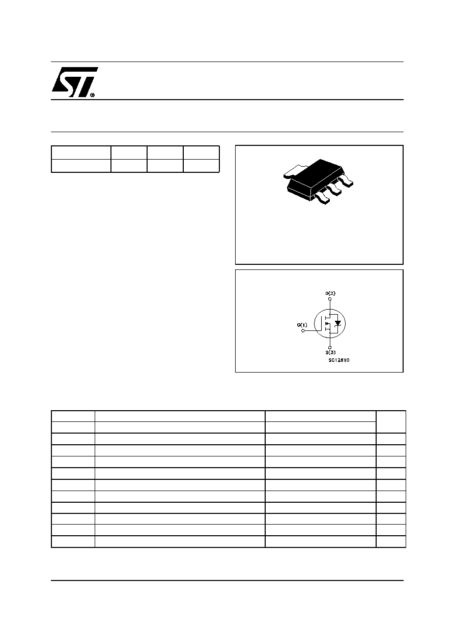
SOT-223
1
2
2
3
INTERNAL SCHEMATIC DIAGRAM
STN3PF06
2/6
THERMAL DATA
ELECTRICAL CHARACTERISTICS (TCASE = 25 ∞C UNLESS OTHERWISE SPECIFIED)
OFF
ON
(1)
DYNAMIC
Rthj-pcb
Thermal Resistance Junction-PC Board Max
50
∞C/W
Rthj-amb
Thermal Resistance Junction-ambient Max
(Surface Mounted)
60
∞C/W
T
l
Maximum Lead Temperature For Soldering Purpose
260
∞C
Symbol
Parameter
Test Conditions
Min.
Typ.
Max.
Unit
V
(BR)DSS
Drain-source
Breakdown Voltage
I
D
= 250 µA, V
GS
= 0
60
V
I
DSS
Zero Gate Voltage
Drain Current (V
GS
= 0)
V
DS
= Max Rating
1
µA
V
DS
= Max Rating, T
C
= 125 ∞C
10
µA
I
GSS
Gate-body Leakage
Current (V
DS
= 0)
V
GS
= ±20V
±100
nA
Symbol
Parameter
Test Conditions
Min.
Typ.
Max.
Unit
V
GS(th)
Gate Threshold Voltage
V
DS
= V
GS
, I
D
= 250µA
2
4
V
R
DS(on)
Static Drain-source On
Resistance
V
GS
= 10V, I
D
= 1.25 A
0.18
0.20
I
D(on)
On State Drain Current
V
DS
> I
D(on)
x R
DS(on)max,
V
GS
= 10V
2.5
A
Symbol
Parameter
Test Conditions
Min.
Typ.
Max.
Unit
g
fs
(1)
Forward Transconductance
V
DS
> I
D(on)
x R
DS(on)max,
I
D
=1.25 A
1.5
S
C
iss
Input Capacitance
V
DS
= 25V, f = 1 MHz, V
GS
= 0
850
pF
C
oss
Output Capacitance
230
pF
C
rss
Reverse Transfer
Capacitance
75
pF

3/6
STN3PF06
ELECTRICAL CHARACTERISTICS (CONTINUED)
SWITCHING ON
SWITCHING OFF
SOURCE DRAIN DIODE
Note: 1. Pulsed: Pulse duration = 300 µs, duty cycle 1.5 %.
2. Pulse width limited by safe operating area.
Symbol
Parameter
Test Conditions
Min.
Typ.
Max.
Unit
t
d(on)
Turn-on Delay Time
V
DD
= 30V, I
D
= 6A
R
G
= 4.7
V
GS
= 10V
(see test circuit, Figure 3)
20
ns
t
r
Rise Time
40
ns
Q
g
Total Gate Charge
V
DD
= 48V, I
D
= 12A,
V
GS
= 10 V
16
21
nC
Q
gs
Gate-Source Charge
4
nC
Q
gd
Gate-Drain Charge
6
nC
Symbol
Parameter
Test Conditions
Min.
Typ.
Max.
Unit
t
d(off)
t
f
Turn-off-Delay Time
Fall Time
V
DD
= 30V, I
D
= 6A,
R
G
= 4.7
,
V
GS
= 10V
(see test circuit, Figure 3)
40
10
ns
ns
t
r(off)
Off-voltage Rise Time
Vclamp =48V, I
D
=12 A
R
G
= 4.7
,
V
GS
= 10V
10
ns
t
f
Fall Time
(see test circuit, Figure 5)
17
ns
t
c
Cross-over Time
30
ns
Symbol
Parameter
Test Conditions
Min.
Typ.
Max.
Unit
I
SD
Source-drain Current
2.5
A
I
SDM
(1)
Source-drain Current (pulsed)
10
A
V
SD
(2)
Forward On Voltage
I
SD
= 2.5A, V
GS
= 0
1.2
V
t
rr
Q
rr
I
RRM
Reverse Recovery Time
Reverse Recovery Charge
Reverse Recovery Current
I
SD
= 12A, di/dt = 100A/µs,
V
DD
= 30V, T
j
= 150∞C
(see test circuit, Figure 5)
100
260
5.2
ns
nC
A
STN3PF06
4/6
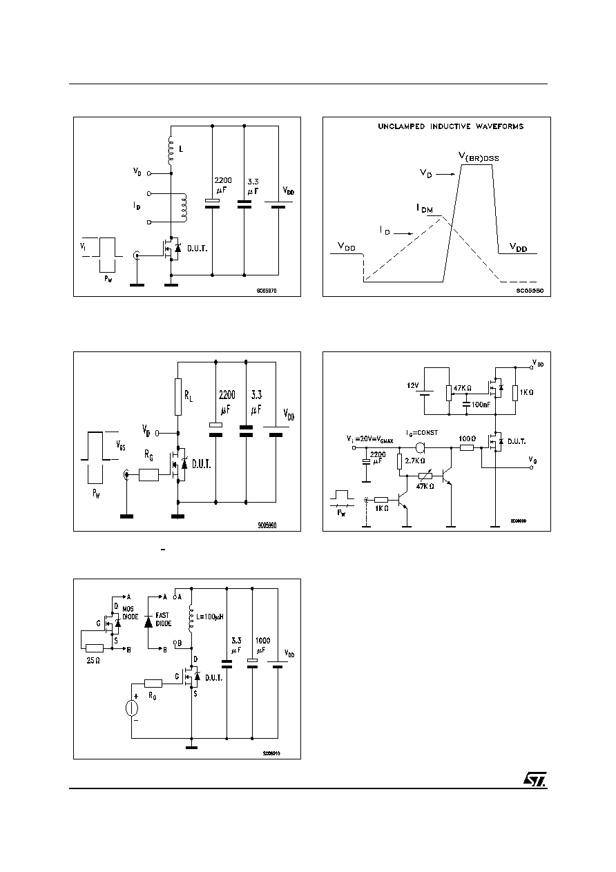
Fig. 5: Test Circuit For Inductive Load Switching
And Diode Recovery Times
Fig. 4: Gate Charge test Circuit
Fig. 2: Unclamped Inductive Waveform
Fig. 1: Unclamped Inductive Load Test Circuit
Fig. 3: Switching Times Test Circuit For
Resistive Load
5/6
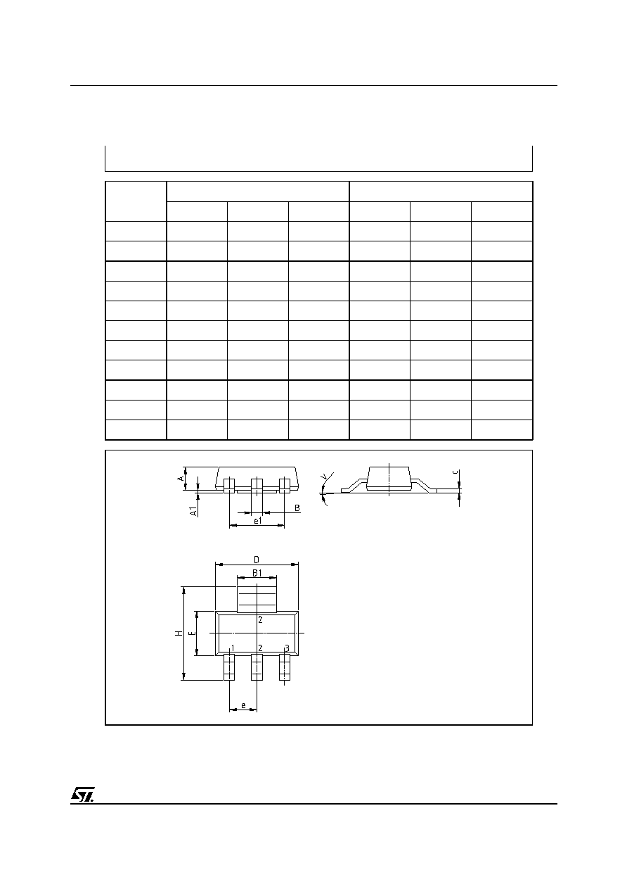
STN3PF06
DIM.
mm
inch
MIN.
TYP.
MAX.
MIN.
TYP.
MAX.
A
1.80
0.071
B
0.60
0.70
0.80
0.024
0.027
0.031
B1
2.90
3.00
3.10
0.114
0.118
0.122
c
0.24
0.26
0.32
0.009
0.010
0.013
D
6.30
6.50
6.70
0.248
0.256
0.264
e
2.30
0.090
e1
4.60
0.181
E
3.30
3.50
3.70
0.130
0.138
0.146
H
6.70
7.00
7.30
0.264
0.276
0.287
V
10
o
10
o
A1
0.02
P008B
SOT-223 MECHANICAL DATA