Rev 1
October 2005
1/10
10
Features
SURFACE MOUNTING DEVICES IN MEDIUM
POWER SOT-223 AND SOT-89 PACKAGE
AVAILABLE IN TAPE & REEL PACKING
IN COMPLIANCE WITH THE 2002/93/EC
EUROPEAN DIRECTIVE
Applications
VOLTAGE REGULATION
RELAY DRIVER
GENERIC SWITCH
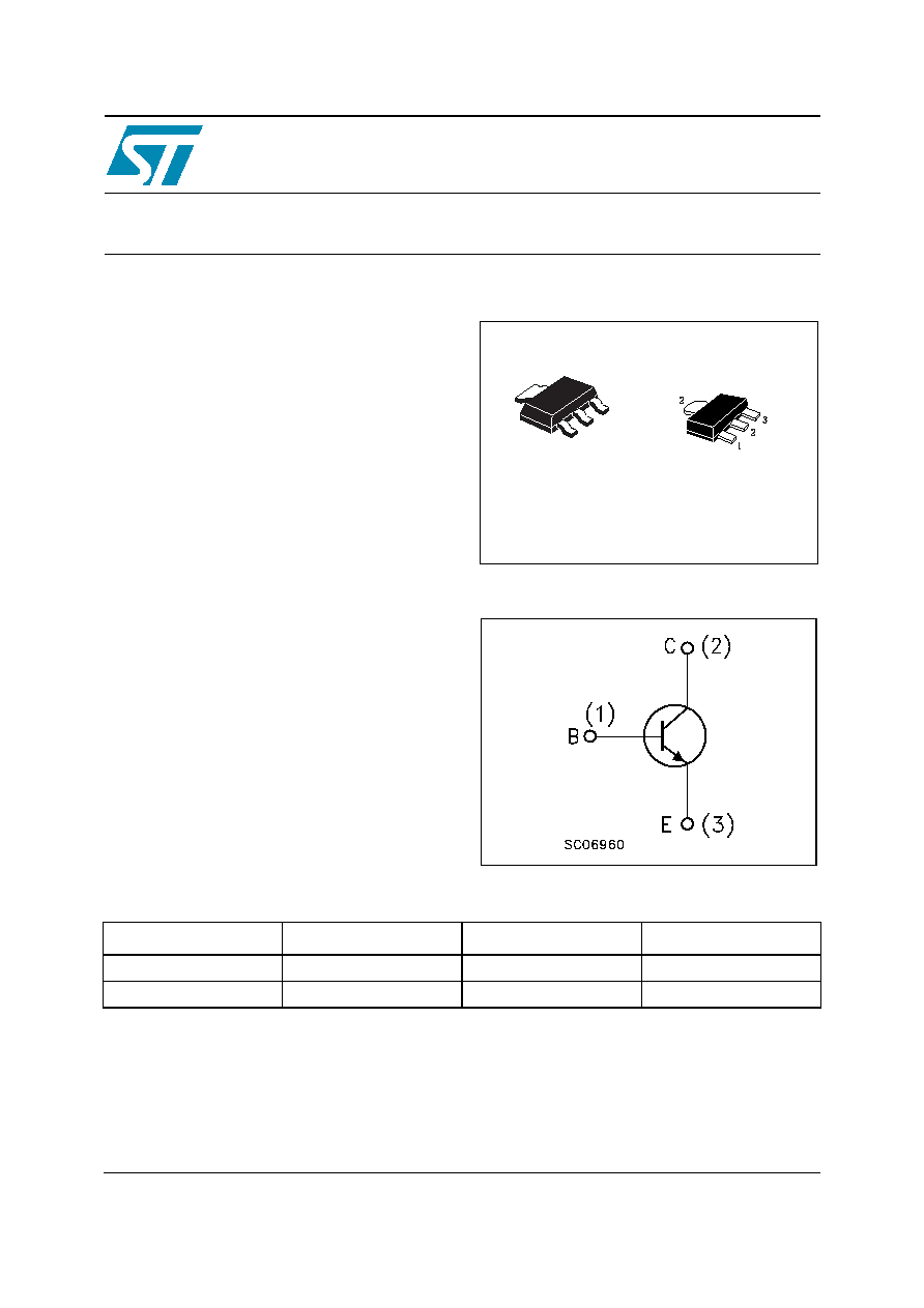
Description
The STF724 and STN724 are PNP transistors
manufactured using planar Technology resulting
in rugged high performance devices.
Order codes
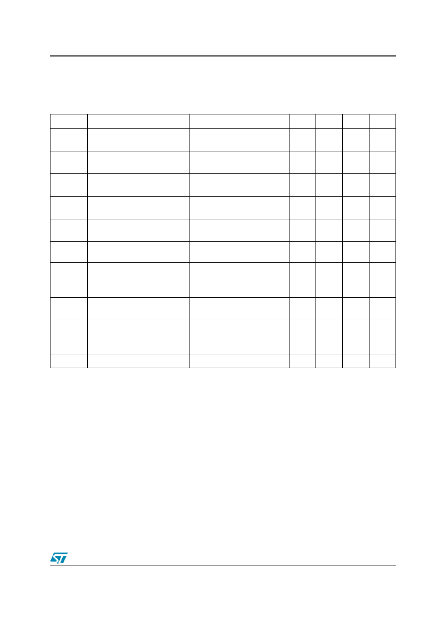
Internal Schematic Diagram
SOT-223
SOT-89
1
2
2
3
Part Number
Marking
Package
Packing
STF724
724
SOT-89
Tape & reel
STN724
N724
SOT-223
Tape & reel
STF724
STN724
NPN MEDIUM POWER TRANSISTORS
www.st.com

1 Absolute Maximum Ratings
STF724 - STN724
2/10
1 Absolute
Maximum
Ratings
Table 1.
Absolute Maximum Rating
Table 2.
Thermal Data
Note: 1 Device mounted on a PCB area of 1 cm
2
.
Symbol
Parameter
Value
Unit
STF724
STN724
V
CBO
Collector-Base Voltage (I
E
= 0)
60
V
V
CEO
Collector-Emitter Voltage (I
B
= 0)
30
V
V
EBO
Collector-Base Voltage (I
C
= 0)
5
V
I
C
Collector Current
3
A
I
CM
Collector Peak Current (t
P
< 5ms)
6
A
I
B
Base Current
1
A
I
BM
Base Peak Current (t
P
< 5ms)
2
A
P
TOT
Total dissipation at T
c
= 25�C
1.4
1.6
W
T
STG
Storage Temperature
-65 to 150
�C
T
J
Max. Operating Junction Temperature
150
Symbol
Parameter
Value
Unit
SOT-89
SOT-223
R
thj-amb
Note: 1
Thermal Resistance Junction-Amb
____________________
Max
89
78
�C/W
STF724 - STN724
2 Electrical Characteristics
3/10
2 Electrical
Characteristics
Table 3.
Electrical Characteristics (T
CASE
= 25�C; unless otherwise specified)
2 Pulsed duration = 300
s, duty cycle
1.5%.
Symbol
Parameter
Test Conditions
Min.
Typ.
Max.
Unit
I
CES
Collector Cut-off Current
(V
BE
= 0)
V
CE
= 60V
10
A
I
CEO
Collector Cut-off Current
(I
B
= 0)
V
CE
= 30V
100
A
I
EBO
Emitter Cut-off Current
(I
C
= 0)
V
EB
= 5V
10
A
V
(BR)CBO
Collector-Base
Breakdown Voltage (I
E
= 0)
I
C
= 100
A
60
V
V
(BR)CEO
Note 2
Collector-Emitter Breakdown
Voltage (I
B
= 0)
I
C
= 10 mA
30
V
V
(BR)EBO
Collector-Emitter Breakdown
Voltage (I
C
= 0)
I
E
= 100
A
5
V
V
CE(sat)
Note 2
Collector-Emitter Saturation
Voltage
I
C
= 1 A I
B
= 50 mA
I
C
= 2 A I
B
= 100 mA
I
C
= 3 A I
B
= 150 mA
0.4
0.7
1.1
V
V
V
V
BE(sat)
Note 2
Base-Emitter Saturation Voltage I
C
= 2 A I
B
= 100 mA
1.2
V
h
FE
DC Current Gain
I
C
= 100 mA V
CE
= 2 V
I
C
= 1 A V
CE
= 2 V
I
C
= 3 A V
CE
= 2 V
100
80
30
300
f
T
Transistor Frequency
V
CE
= 10 V I
c
= 0.1 A
100
MHz
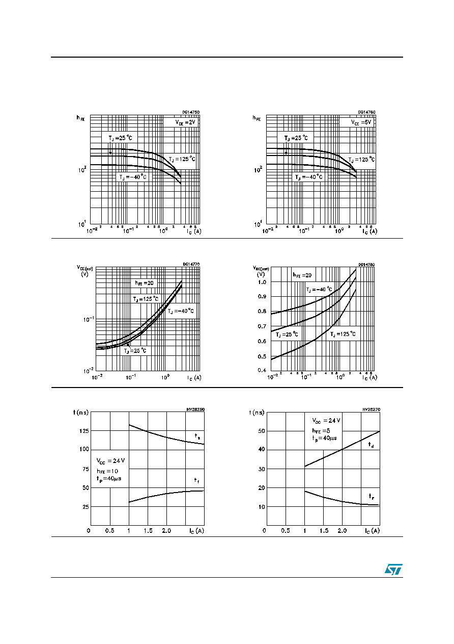
2 Electrical Characteristics
STF724 - STN724
4/10
2.1 Electrical
characteristics
(curve)
Figure 1.
DC Current Gain
Figure 2.
DC Current Gain
Figure 3.
Collector-emitter saturation voltage Figure 4.
Base-emitter saturation voltage
Figure 5.
Switching times on resistive load
Figure 6.
Switching times resistive on load
STF724 - STN724
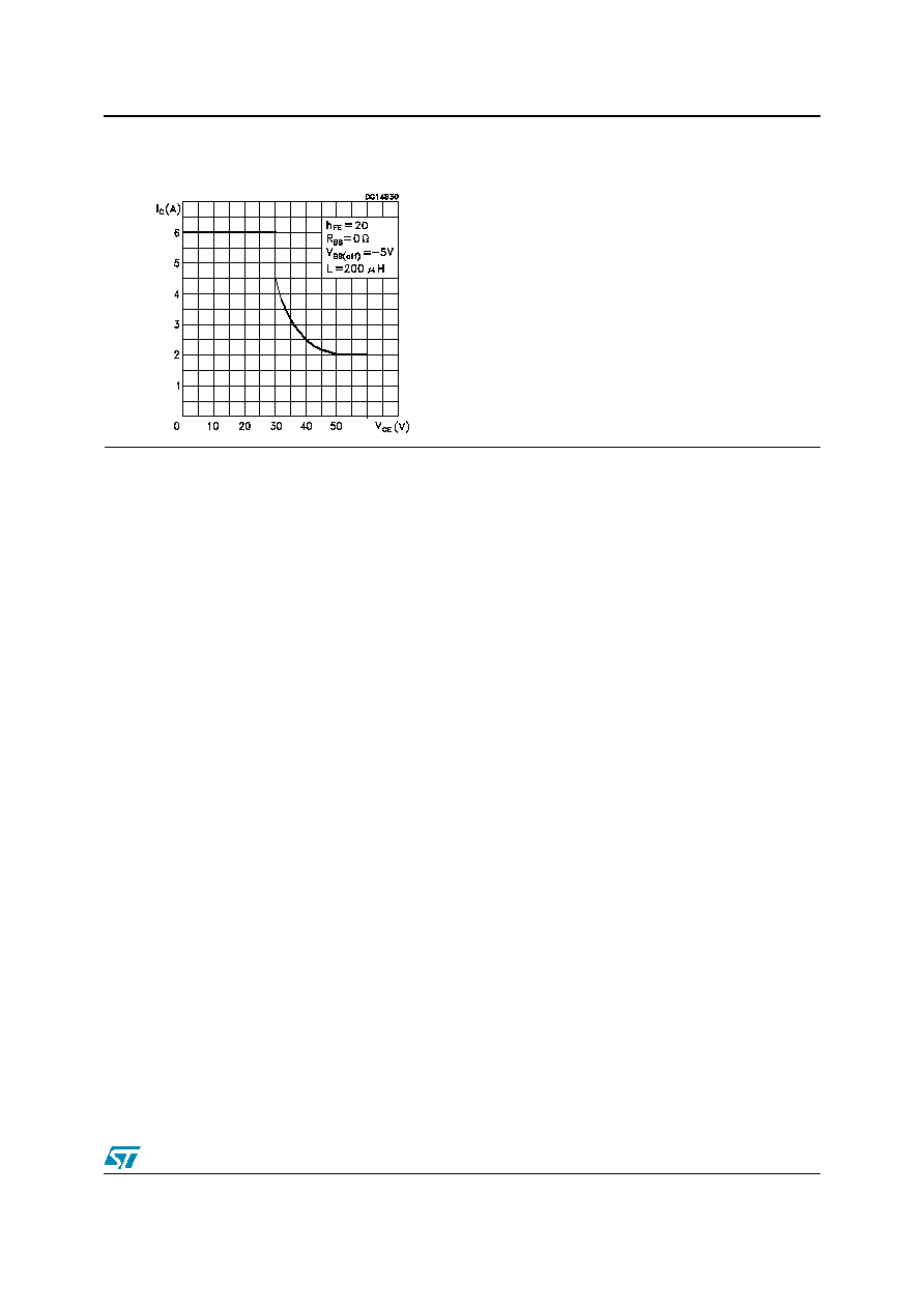
2 Electrical Characteristics
5/10
Figure 7.
Reverse biased area