 | –≠–ª–µ–∫—Ç—Ä–æ–Ω–Ω—ã–π –∫–æ–º–ø–æ–Ω–µ–Ω—Ç: STN7NF10 | –°–∫–∞—á–∞—Ç—å:  PDF PDF  ZIP ZIP |

1/8
December 2002
STN7NF10
N-CHANNEL 100V - 0.055
- 5A SOT-223
LOW GATE CHARGE STripFETTM II POWER MOSFET
s
TYPICAL R
DS
(on) = 0.055
s
APPLICATION ORIENTED
CHARACTERIZATION
DESCRIPTION
This Power MOSFET series realized with STMicro-
electronics unique STripFET process has specifical-
ly been designed to minimize input capacitance and
gate charge. It is therefore suitable as primary
switch in advanced high-efficiency isolated DC-DC
converters for Telecom and Computer application. It
is also intended for any application with low gate
charge drive requirements.
APPLICATIONS
s
HIGH-EFFICIENCY DC-DC CONVERTERS
s
UPS AND MOTOR CONTROL
ABSOLUTE MAXIMUM RATINGS
(
q
) Pulse width limited by safe operating area
TYPE
V
DSS
R
DS(on)
I
D
STN7NF10
100 V
< 0.065
5 A
Symbol
Parameter
Value
Unit
V
DS
Drain-source Voltage (V
GS
= 0)
100
V
V
DGR
Drain-gate Voltage (R
GS
= 20 k
)
100
V
V
GS
Gate- source Voltage
±20
V
I
D
Drain Current (continuous) at T
C
= 25∞C
5
A
I
D
Drain Current (continuous) at T
C
= 100∞C
3.4
A
I
DM
( )
Drain Current (pulsed)
20
A
P
TOT
Total Dissipation at T
C
= 25∞C
3.3
W
Derating Factor
0.026
W/∞C
T
stg
Storage Temperature
≠55 to 150
∞C
T
j
Operating Junction Temperature
SOT-223
1
2
2
3
INTERNAL SCHEMATIC DIAGRAM
STN7NF10
2/8
THERMAL DATA
Note: (*) When mounted on 1 in
2
FR-4 BOARD,2 oz Cu, t<10s.
Note: (**) When mounted on minimum footprint.
ELECTRICAL CHARACTERISTICS (T
CASE
= 25 ∞C UNLESS OTHERWISE SPECIFIED)
OFF
ON (1)
DYNAMIC
Rthj-PCB
Thermal Resistance Junction-PCB Max(*)
38
∞C/W
Rthj-PCB
Thermal Resistance Junction-PCB Max(**)
100
∞C/W
T
l
Maximum Lead Temperature For Soldering Purpose
(1.6 mm from case,for 10s)
260
∞C
Symbol
Parameter
Test Conditions
Min.
Typ.
Max.
Unit
V
(BR)DSS
Drain-source
Breakdown Voltage
I
D
= 250 µA, V
GS
= 0
100
V
I
DSS
Zero Gate Voltage
Drain Current (V
GS
= 0)
V
DS
= Max Rating
1
µA
V
DS
= Max Rating, T
C
= 125 ∞C
10
µA
I
GSS
Gate-body Leakage
Current (V
DS
= 0)
V
GS
= ±20V
±100
nA
Symbol
Parameter
Test Conditions
Min.
Typ.
Max.
Unit
V
GS(th)
Gate Threshold Voltage
V
DS
= V
GS
, I
D
= 250µA
2
3
4
V
R
DS(on)
Static Drain-source On
Resistance
V
GS
= 10V, I
D
= 1.5 A
0.055
0.065
Symbol
Parameter
Test Conditions
Min.
Typ.
Max.
Unit
g
fs
(1)
Forward Transconductance
V
DS
= 15 V , I
D
= 1.5 A
12
S
C
iss
Input Capacitance
V
DS
= 25 V, f = 1 MHz, V
GS
= 0
870
pF
C
oss
Output Capacitance
125
pF
C
rss
Reverse Transfer
Capacitance
52
pF
3/8
STN7NF10
ELECTRICAL CHARACTERISTICS (CONTINUED)
SWITCHING ON
SWITCHING OFF
SOURCE DRAIN DIODE
Note: 1. Pulsed: Pulse duration = 300 µs, duty cycle 1.5 %.
2. Pulse width limited by safe operating area.
Symbol
Parameter
Test Conditions
Min.
Typ.
Max.
Unit
t
d(on)
Turn-on Delay Time
V
DD
= 50 V, I
D
= 12 A
R
G
= 4.7
V
GS
= 10 V
(see test circuit, Figure 3)
58
ns
t
r
Rise Time
45
ns
Q
g
Q
gs
Q
gd
Total Gate Charge
Gate-Source Charge
Gate-Drain Charge
V
DD
= 80 V, I
D
= 24 A,
V
GS
= 10 V
30
6
10
41
nC
nC
nC
Symbol
Parameter
Test Conditions
Min.
Typ.
Max.
Unit
t
d(off)
t
f
Turn-off-Delay Time
Fall Time
V
DD
= 50 V, I
D
= 12 A,
R
G
= 4.7
,
V
GS
= 10V
(see test circuit, Figure 3)
49
17
ns
ns
Symbol
Parameter
Test Conditions
Min.
Typ.
Max.
Unit
I
SD
Source-drain Current
5
A
I
SDM
(1)
Source-drain Current (pulsed)
20
A
V
SD
(2)
Forward On Voltage
I
SD
= 5 A, V
GS
= 0
1.3
V
t
rr
Q
rr
I
RRM
Reverse Recovery Time
Reverse Recovery Charge
Reverse Recovery Current
I
SD
= 5 A, di/dt = 100A/µs,
V
DD
= 30 V, T
j
= 150∞C
(see test circuit, Figure 5)
100
375
7.5
ns
nC
A
STN7NF10
4/8
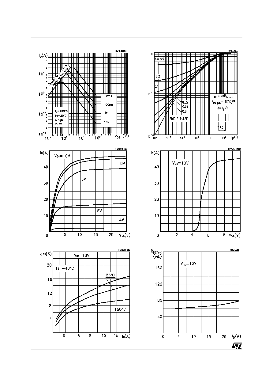
Thermal Impedence
Safe Operating Area
Transconductance
Static Drain-source On Resistance
Output Characteristics
Transfer Characteristics
5/8
STN7NF10
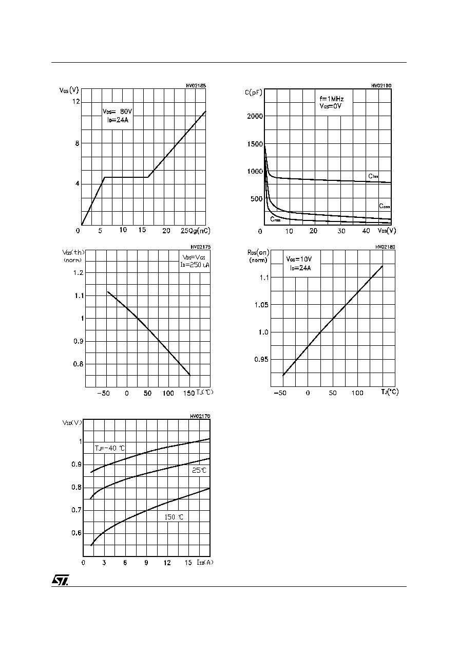
Gate Charge vs Gate-source Voltage
Capacitance Variations
Normalized On Resistance vs Temperature
Normalized Gate Thereshold Voltage vs Temp.
Source-drain Diode Forward Characteristics