 | –≠–ª–µ–∫—Ç—Ä–æ–Ω–Ω—ã–π –∫–æ–º–ø–æ–Ω–µ–Ω—Ç: STP20N10 | –°–∫–∞—á–∞—Ç—å:  PDF PDF  ZIP ZIP |

STP20N10
N - CHANNEL ENHANCEMENT MODE
POWER MOS TRANSISTOR
s
TYPICAL R
DS(on)
= 0.09
s
AVALANCHE RUGGED TECHNOLOGY
s
100% AVALANCHE TESTED
s
REPETITIVE AVALANCHE DATA AT 100
o
C
s
LOW GATE CHARGE
s
HIGH CURRENT CAPABILITY
s
175
o
C OPERATING TEMPERATURE
s
APPLICATION ORIENTED
CHARACTERIZATION
APPLICATIONS
s
HIGH CURRENT, HIGH SPEED SWITCHING
s
SOLENOID AND RELAY DRIVERS
s
REGULATORS
s
DC-DC & DC-AC CONVERTERS
s
MOTOR CONTROL, AUDIO AMPLIFIERS
s
AUTOMOTIVE ENVIRONMENT (INJECTION,
ABS, AIR-BAG, LAMPDRIVERS, Etc.)
INTERNAL SCHEMATIC DIAGRAM
TYPE
V
DSS
R
DS ( on)
I
D
STP20N10
100 V
< 0. 12
20 A
1
2
3
TO-220
December 1996
ABSOLUTE MAXIMUM RATINGS
Symbol
Parameter
Value
Uni t
V
D S
Drain-source Voltage (V
GS
= 0)
100
V
V
DG R
Drain- gate Voltage (R
GS
= 20 k
)
100
V
V
GS
Gate-source Voltage
±
20
V
I
D
Drain Current (cont inuous) at T
c
= 25
o
C
20
A
I
D
Drain Current (cont inuous) at T
c
= 100
o
C
14
A
I
D M
(
∑
)
Drain Current (pulsed)
80
A
P
tot
Total Dissipation at T
c
= 25
o
C
105
W
Derating Factor
0.7
W/
o
C
T
stg
St orage Temperat ure
-65 to 175
o
C
T
j
Max. Operat ing Junction Temperature
175
o
C
(
∑
) Pulse width limited by safe operating area
1/9
THERMAL DATA
R
thj-cas e
R
thj- amb
R
thj- amb
T
l
Thermal Resist ance Junct ion-case
Max
Thermal Resist ance Junct ion-ambient
Max
Thermal Resist ance Case-sink
Typ
Maximum Lead Temperature For Soldering Purpose
1.43
62.5
0.5
300
o
C/ W
o
C/ W
o
C/ W
o
C
AVALANCHE CHARACTERISTICS
Symbol
Parameter
Max Value
Uni t
I
A R
Avalanche Current, Repetitive or Not-Repetitive
(pulse width limited by T
j
max,
< 1%)
20
A
E
AS
Single Pulse Avalanche Energy
(st arting T
j
= 25
o
C, I
D
= I
AR
, V
D D
= 25 V)
60
mJ
E
AR
Repet itive Avalanche Energy
(pulse width limited by T
j
max,
< 1%)
15
mJ
I
A R
Avalanche Current, Repetitive or Not-Repetitive
(T
c
= 100
o
C, pulse width limited by T
j
max,
< 1%)
14
A
ELECTRICAL CHARACTERISTICS (T
case
= 25
o
C unless otherwise specified)
OFF
Symbol
Parameter
Test Condi tions
Mi n.
Typ.
Max.
Unit
V
( BR)DSS
Drain-source
Breakdown Voltage
I
D
= 250
µ
A
V
G S
= 0
100
V
I
DS S
Zero Gate Volt age
Drain Current (V
GS
= 0)
V
DS
= Max Rating
V
DS
= Max Rating x 0.8
T
c
= 125
o
C
1
10
µ
A
µ
A
I
G SS
Gate-body Leakage
Current (V
D S
= 0)
V
GS
=
±
20 V
±
100
nA
ON (
)
Symbol
Parameter
Test Condi tions
Mi n.
Typ.
Max.
Unit
V
G S(th)
Gate Threshold Voltage V
DS
= V
GS
I
D
= 250
µ
A
2
2.9
4
V
R
DS( on)
St atic Drain-source On
Resist ance
V
GS
= 10V
I
D
= 10 A
0.09
0. 12
I
D( on)
On St ate Drain Current
V
DS
> I
D( on)
x R
D S(on) max
V
GS
= 10 V
20
A
DYNAMIC
Symbol
Parameter
Test Condi tions
Mi n.
Typ.
Max.
Unit
g
fs
(
)
Forward
Transconductance
V
DS
> I
D( on)
x R
D S(on) max
I
D
= 10 A
7
12
S
C
iss
C
oss
C
rss
I nput Capacitance
Output Capacit ance
Reverse Transfer
Capacitance
V
DS
= 25 V
f = 1 MHz
V
G S
= 0
800
200
40
1100
300
60
pF
pF
pF
STP20N10
2/9

ELECTRICAL CHARACTERISTICS (continued)
SWITCHING ON
Symbol
Parameter
Test Condi tions
Mi n.
Typ.
Max.
Unit
t
d(on)
t
r
Turn-on Time
Rise Time
V
DD
= 30 V
I
D
= 3 A
R
G
= 50
V
GS
= 10 V
(see test circuit, figure 3)
25
75
35
110
ns
ns
(di/dt)
on
Turn-on Current Slope
V
DD
= 80 V
I
D
= 20 A
R
G
= 50
V
GS
= 10 V
(see test circuit, figure 5)
300
A/
µ
s
Q
g
Q
gs
Q
gd
Total Gate Charge
Gate-Source Charge
Gate-Drain Charge
V
DD
= 80 V
I
D
= 20 A
V
GS
= 10 V
30
9
11
45
nC
nC
nC
SWITCHING OFF
Symbol
Parameter
Test Condi tions
Mi n.
Typ.
Max.
Unit
t
r(Vof f)
t
f
t
c
Of f-voltage Rise Time
Fall Time
Cross-over Time
V
DD
= 80 V
I
D
= 20 A
R
G
= 50
V
GS
= 10 V
(see test circuit, figure 5)
70
55
130
100
80
185
ns
ns
ns
SOURCE DRAIN DIODE
Symbol
Parameter
Test Condi tions
Mi n.
Typ.
Max.
Unit
I
S D
I
SD M
(
∑
)
Source-drain Current
Source-drain Current
(pulsed)
20
80
A
A
V
S D
(
)
Forward On Volt age
I
SD
= 20 A
V
G S
= 0
1.6
V
t
rr
Q
rr
I
RRM
Reverse Recovery
Time
Reverse Recovery
Charge
Reverse Recovery
Current
I
SD
= 20 A
di/dt = 100 A/
µ
s
V
DD
= 20 V
T
j
= 150
o
C
(see test circuit, figure 5)
125
0.44
7
ns
µ
C
A
(
) Pulsed: Pulse duration = 300
µ
s, duty cycle 1.5 %
(
∑
) Pulse width limited by safe operating area
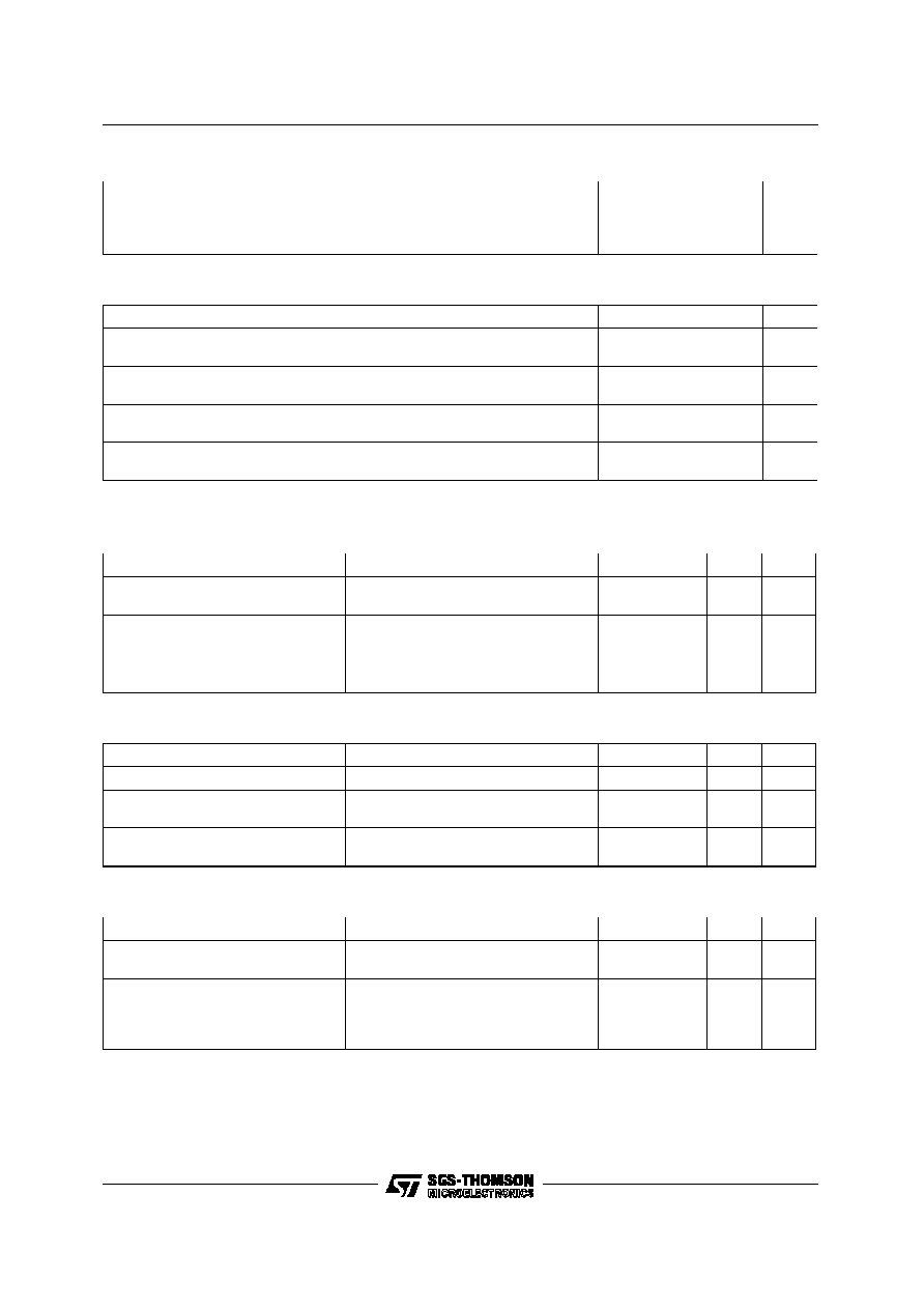
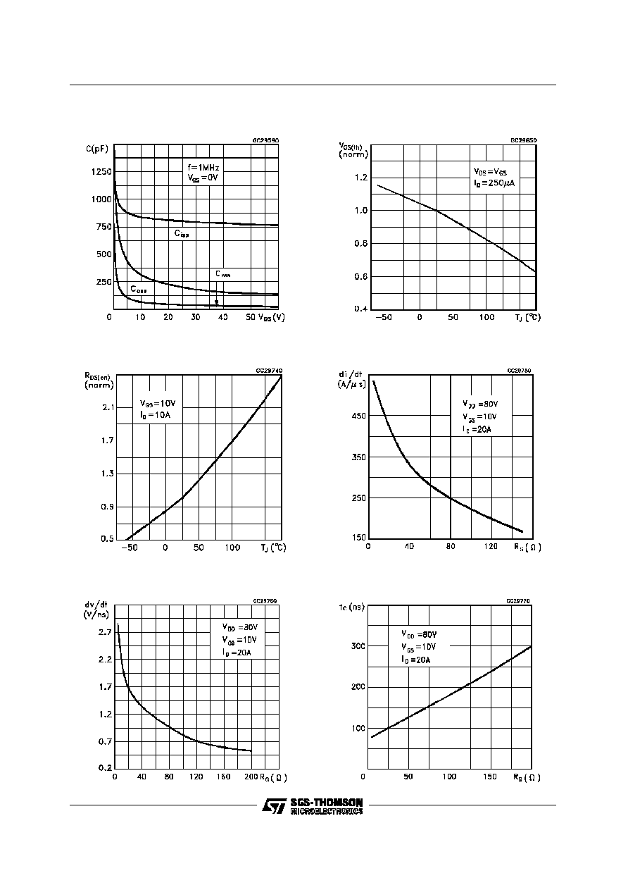
Safe Operating Areas
Thermal Impedance
STP20N10
3/9
Derating Curve
Transfer Characteristics
Static Drain-source On Resistance
Output Characteristics
Transconductance
Gate Charge vs Gate-source Voltage
STP20N10
4/9
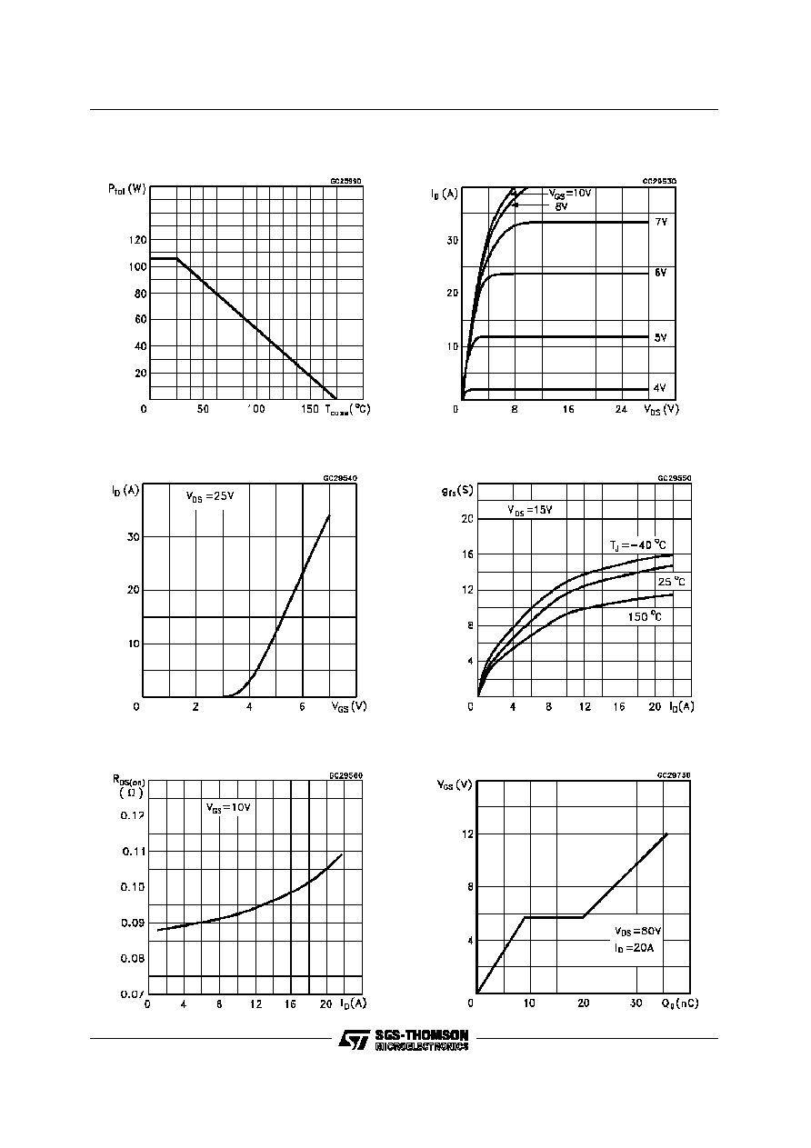
Capacitance Variations
Normalized Gate Threshold Voltage vs
Temperature
Normalized On Resistance vs Temperature
Turn-on Current Slope
Cross-over Time
Turn-off Drain-source Voltage Slope
STP20N10
5/9
Switching Safe Operating Area
Accidental Overload Area
Source-drain Diode Forward Characteristics
Fig. 1: Unclamped Inductive Load Test Circuits
Fig. 2: Unclamped Inductive Waveforms
STP20N10
6/9
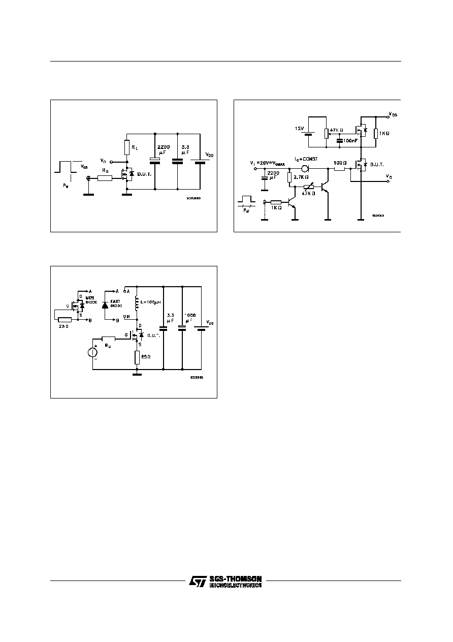
Fig. 4: Gate Charge Test Circuit
Fig. 5: Test Circuit For Inductive Load Switching
And Diode Recovery Times
Fig. 3: Switching Times Test Circuits For
Resistive Load
STP20N10
7/9
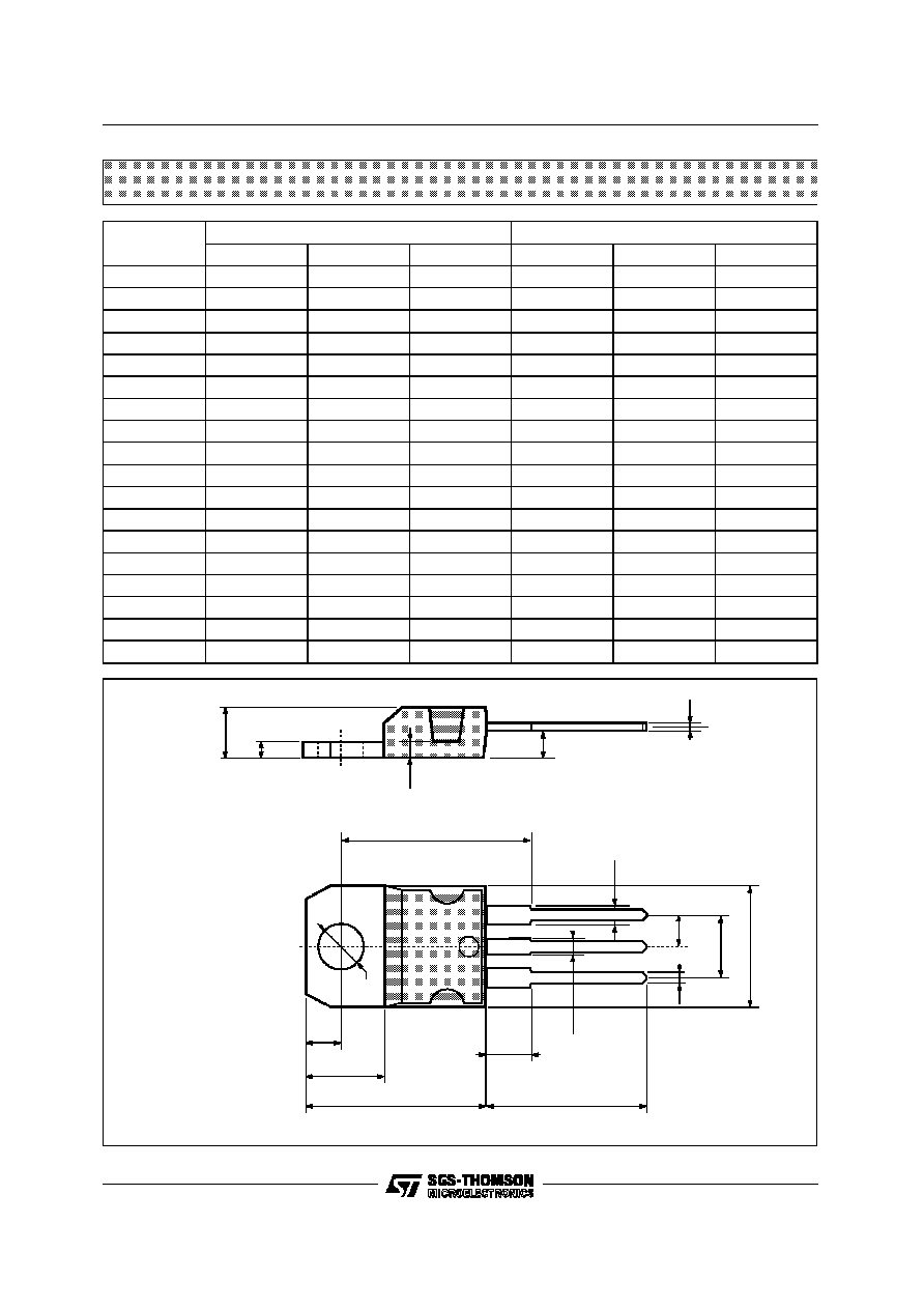
DIM.
mm
inch
MIN.
TYP.
MAX.
MIN.
TYP.
MAX.
A
4.40
4.60
0.173
0.181
C
1.23
1.32
0.048
0.051
D
2.40
2.72
0.094
0.107
D1
1.27
0.050
E
0.49
0.70
0.019
0.027
F
0.61
0.88
0.024
0.034
F1
1.14
1.70
0.044
0.067
F2
1.14
1.70
0.044
0.067
G
4.95
5.15
0.194
0.203
G1
2.4
2.7
0.094
0.106
H2
10.0
10.40
0.393
0.409
L2
16.4
0.645
L4
13.0
14.0
0.511
0.551
L5
2.65
2.95
0.104
0.116
L6
15.25
15.75
0.600
0.620
L7
6.2
6.6
0.244
0.260
L9
3.5
3.93
0.137
0.154
DIA.
3.75
3.85
0.147
0.151
L6
A
C
D
E
D1
F
G
L7
L2
Dia.
F1
L5
L4
H2
L9
F2
G1
TO-220 MECHANICAL DATA
P011C
STP20N10
8/9

Information furnished is believed to be accurate and reliable. However, SGS-THOMSON Microelectronics assumes no responsability for the
consequences of use of such information nor for any infringement of patents or other rights of third parties which may results from its use. No
license is granted by implication or otherwise under any patent or patent rights of SGS-THOMSON Microelectronics. Specifications mentioned
in this publication are subject to change without notice. This publication supersedes and replaces all information previously supplied.
SGS-THOMSON Microelectronics products are not authorized for use as critical components in life support devices or systems without express
written approval of SGS-THOMSON Microelectonics.
©
1996 SGS-THOMSON Microelectronics - Printed in Italy - All Rights Reserved
SGS-THOMSON Microelectronics GROUP OF COMPANIES
Australia - Brazil - Canada - China - France - Germany - Hong Kong - Italy - Japan - Korea - Malaysia - Malta - Morocco - The Netherlands -
Singapore - Spain - Sweden - Switzerland - Taiwan - Thailand - United Kingdom - U.S.A
.
STP20N10
9/9