 | –≠–ª–µ–∫—Ç—Ä–æ–Ω–Ω—ã–π –∫–æ–º–ø–æ–Ω–µ–Ω—Ç: STP45N10 | –°–∫–∞—á–∞—Ç—å:  PDF PDF  ZIP ZIP |
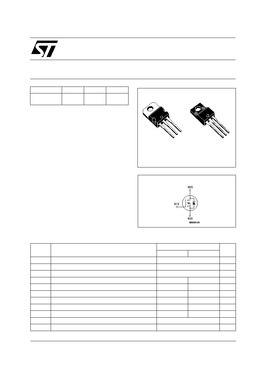
STP45N10
STP45N10FI
N - CHANNEL 100V - 0.027
- 45A - TO-220/TO-220FI
POWER MOS TRANSISTOR
s
TYPICAL R
DS(on)
= 0.027
s
AVALANCHE RUGGED TECHNOLOGY
s
100% AVALANCHE TESTED
s
REPETITIVE AVALANCHE DATA AT 100
o
C
s
LOW GATE CHARGE
s
HIGH CURRENT CAPABILITY
s
175
o
C OPERATING TEMPERATURE
s
APPLICATION ORIENTED
CHARACTERIZATION
APPLICATIONS
s
HIGH CURRENT, HIGH SPEED SWITCHING
s
SOLENOID AND RELAY DRIVERS
s
DC-DC & DC-AC CONVERTERS
s
AUTOMOTIVE ENVIRONMENT (INJECTION,
ABS, AIR-BAG, LAMP DRIVERS. Etc.)
Æ
INTERNAL SCHEMATIC DIAGRAM
ABSOLUTE MAXIMUM RATINGS
Symbol
Parameter
Value
Unit
STP45N10
STP45N10FI
V
DS
Drain-source Voltage (V
GS
= 0)
100
V
V
DGR
Drain- gate Voltage (R
GS
= 20 k
)
100
V
V
GS
Gate-source Voltage
±
25
V
I
D
Drain Current (continuous) at T
c
= 25
o
C
45
24
A
I
D
Drain Current (continuous) at T
c
= 100
o
C
32
17
A
I
DM
(
∑
)
Drain Current (pulsed)
180
180
A
P
tot
Total Dissipation at T
c
= 25
o
C
150
45
W
Derating Factor
1
0.3
W/
o
C
V
ISO
Insulation Withstand Voltage (DC)
2000
V
T
stg
Storage Temperature
-65 to 175
o
C
T
j
Max. Operating Junction Temperature
175
o
C
TYPE
V
DSS
R
DS(on)
I
D
STP45N10
STP45N10FI
100 V
100 V
< 0.035
< 0.035
45 A
24 A
June 1998
1
2
3
TO-220 ISOWATT220
1
2
3
1/10
THERMAL DATA
TO220
ISOWATT220
R
thj-case
Thermal Resistance Junction-case Max
1
3.33
o
C/W
R
thj-amb
R
thc-sink
T
l
Thermal Resistance Junction-ambient Max
Thermal Resistance Case-sink Typ
Maximum Lead Temperature For Soldering Purpose
62.5
0.5
300
o
C/W
o
C/W
o
C
AVALANCHE CHARACTERISTICS
Symbol
Parameter
Max Value
Unit
I
AR
Avalanche Current, Repetitive or Not-Repetitive
(pulse width limited by T
j
max,
< 1%)
45
A
E
AS
Single Pulse Avalanche Energy
(starting T
j
= 25
o
C, I
D
= I
AR
, V
DD
= 25 V)
400
mJ
ELECTRICAL CHARACTERISTICS (T
case
= 25
o
C unless otherwise specified)
OFF
Symbol
Parameter
Test Conditions
Min.
Typ.
Max.
Unit
V
(BR)DSS
Drain-source
Breakdown Voltage
I
D
= 250
µ
A V
GS
= 0
100
V
I
DSS
Zero Gate Voltage
Drain Current (V
GS
= 0)
V
DS
= Max Rating
V
DS
= Max Rating x 0.8
V
DS
= Max Rating x 0.8 T
c
= 125
o
C
10
1
50
µ
A
µ
A
I
GSS
Gate-Source Leakage
Current (V
DS
= 0)
V
GS
=
±
20 V
±
100
mA
ON (
)
Symbol
Parameter
Test Conditions
Min.
Typ.
Max.
Unit
V
GS(th)
Gate Threshold
Voltage
V
DS
= V
GS
I
D
= 250
µ
A
2
3
4
V
R
DS(on)
Static Drain-source On
Resistance
V
GS
= 10 V I
D
= 22.5 A
V
GS
= 10 V I
D
= 22.5 A T
c
= 100
o
C
0.027
0.035
0.07
I
D(on )
On State Drain Current V
DS
> I
D(on)
x R
DS(on)max
V
GS
= 10 V
45
A
DYNAMIC
Symbol
Parameter
Test Conditions
Min.
Typ.
Max.
Unit
g
fs
(
)
Forward
Transconductance
V
DS
> I
D(on)
x R
DS(on)max
I
D
= 22.5 A
20
40
S
C
iss
C
oss
C
rss
Input Capacitance
Output Capacitance
Reverse Transfer
Capacitance
V
DS
= 25 V f = 1 MHz V
GS
= 0
4100
600
150
5200
800
220
pF
pF
pF
STP45N10/FI
2/10
ELECTRICAL CHARACTERISTICS (continued)
SWITCHING ON
Symbol
Parameter
Test Conditions
Min.
Typ.
Max.
Unit
t
d(on)
t
r
Turn-on Time
Rise Time
V
DD
= 50 V I
D
= 22.5
A
R
G
= 4.7
V
GS
= 10 V
25
75
35
105
ns
ns
(di/dt)
o n
Turn-on Current Slope
V
DD
= 80 V I
D
= 45 A
R
G
= 47
V
GS
= 10 V
400
A/
µ
s
Q
g
Q
gs
Q
gd
Total Gate Charge
Gate-Source Charge
Gate-Drain Charge
V
DD
= 80 V I
D
=45 A V
GS
= 10 V
120
20
50
170
nC
nC
nC
SWITCHING OFF
Symbol
Parameter
Test Conditions
Min.
Typ.
Max.
Unit
t
r(Voff)
t
f
t
c
Off-voltage Rise Time
Fall Time
Cross-over Time
V
DD
= 80 V I
D
= 45 A
R
G
= 4.7
V
GS
= 10 V
30
35
65
45
50
95
ns
ns
ns
SOURCE DRAIN DIODE
Symbol
Parameter
Test Conditions
Min.
Typ.
Max.
Unit
I
SD
I
SDM
(
∑
)
Source-drain Current
Source-drain Current
(pulsed)
45
180
A
A
V
SD
(
)
Forward On Voltage
I
SD
= 45 A V
GS
= 0
1.5
V
t
rr
Q
rr
I
RRM
Reverse Recovery
Time
Reverse Recovery
Charge
Reverse Recovery
Current
I
SD
= 45 A di/dt = 100 A/
µ
s
V
DD
= 30 V T
j
= 150
o
C
200
0.14
14
ns
µ
C
A
(
) Pulsed: Pulse duration = 300
µ
s, duty cycle 1.5 %
(
∑
) Pulse width limited by safe operating area
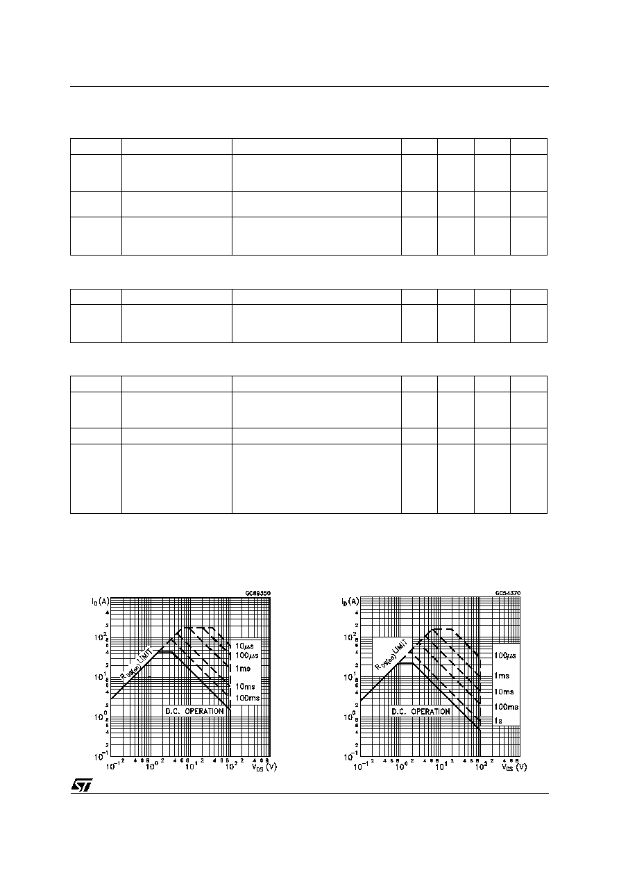
Safe Operating Area for TO-220
Safe Operating Area for ISOWATT220
STP45N10/FI
3/10
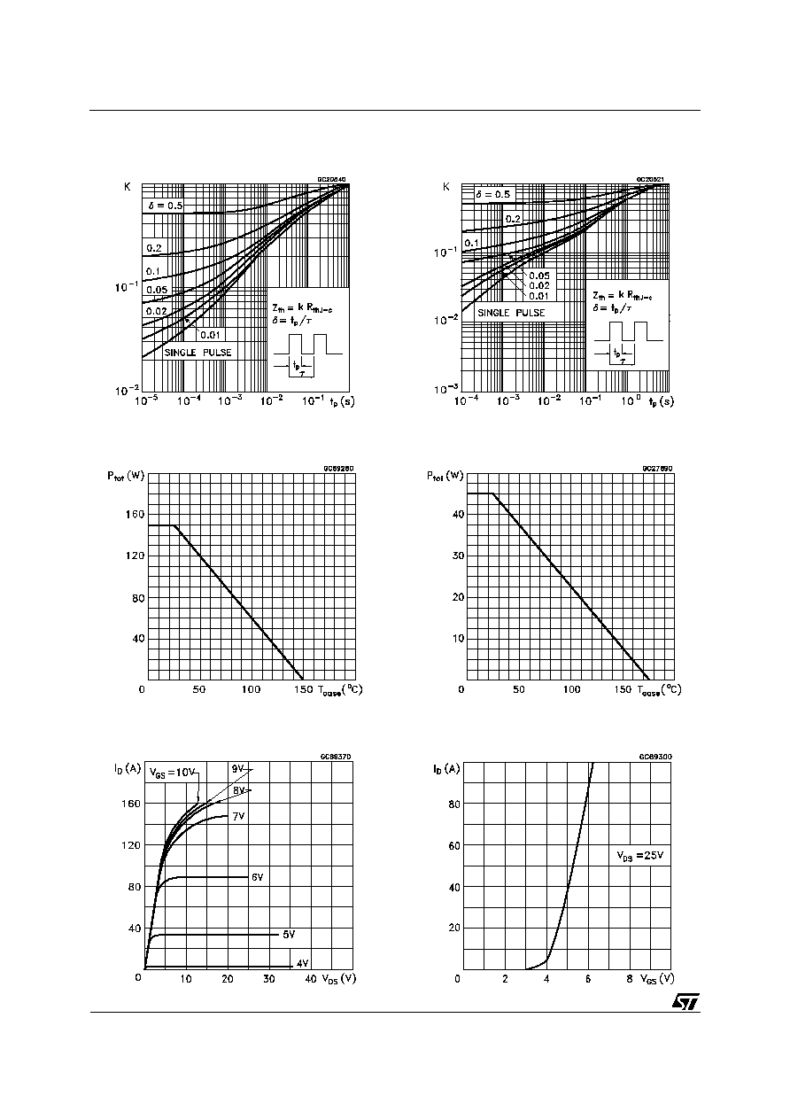
Thermal Impedance for TO-220
Derating Curve for TO-220
Output Characteristics
Thermal Impedance for ISOWATT220
Derating Curve for ISOWATT220
Transfer Characteristics
STP45N10/FI
4/10
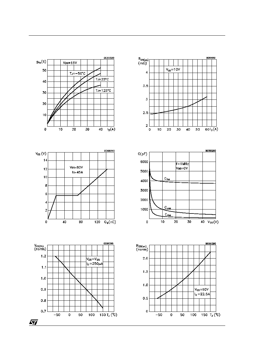
Transconductance
Gate Charge vs Gate-source Voltage
Normalized Gate Threshold Voltage vs
Temperature
Static Drain-source On Resistance
Capacitance Variations
Normalized On Resistance vs Temperature
STP45N10/FI
5/10
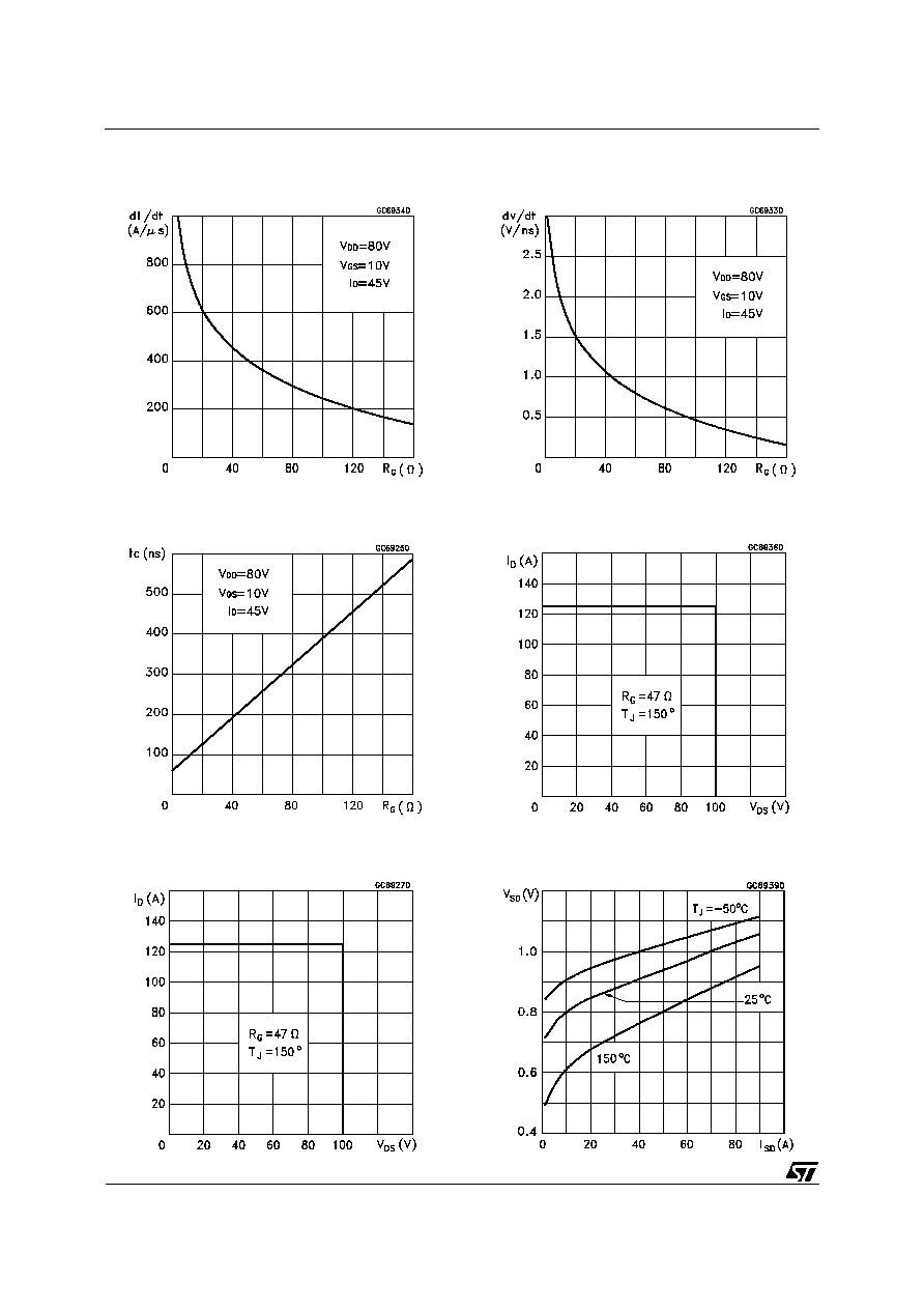
Turn-on Current Slope
Cross-over Time
Accidental Overload Area
Turn-off Drain-source Voltage Slope
Switching Safe Operating Area
Source-drain Diode Forward Characteristics
STP45N10/FI
6/10
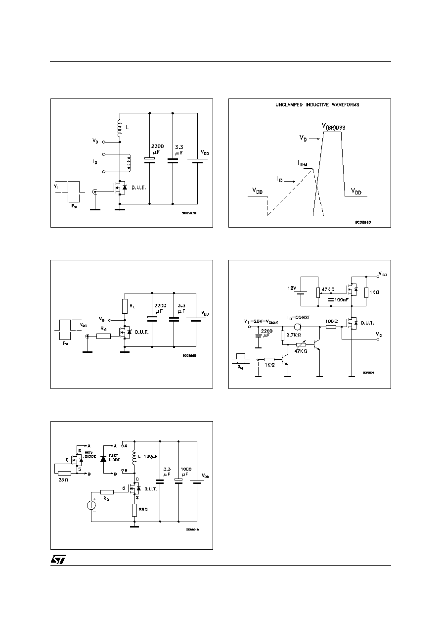
Fig. 1: Unclamped Inductive Load Test Circuit
Fig. 3: Switching Times Test Circuits For
Resistive Load
Fig. 2: Unclamped Inductive Waveform
Fig. 4: Gate Charge test Circuit
Fig. 5: Test Circuit For Inductive Load Switching
And Diode Recovery Times
STP45N10/FI
7/10
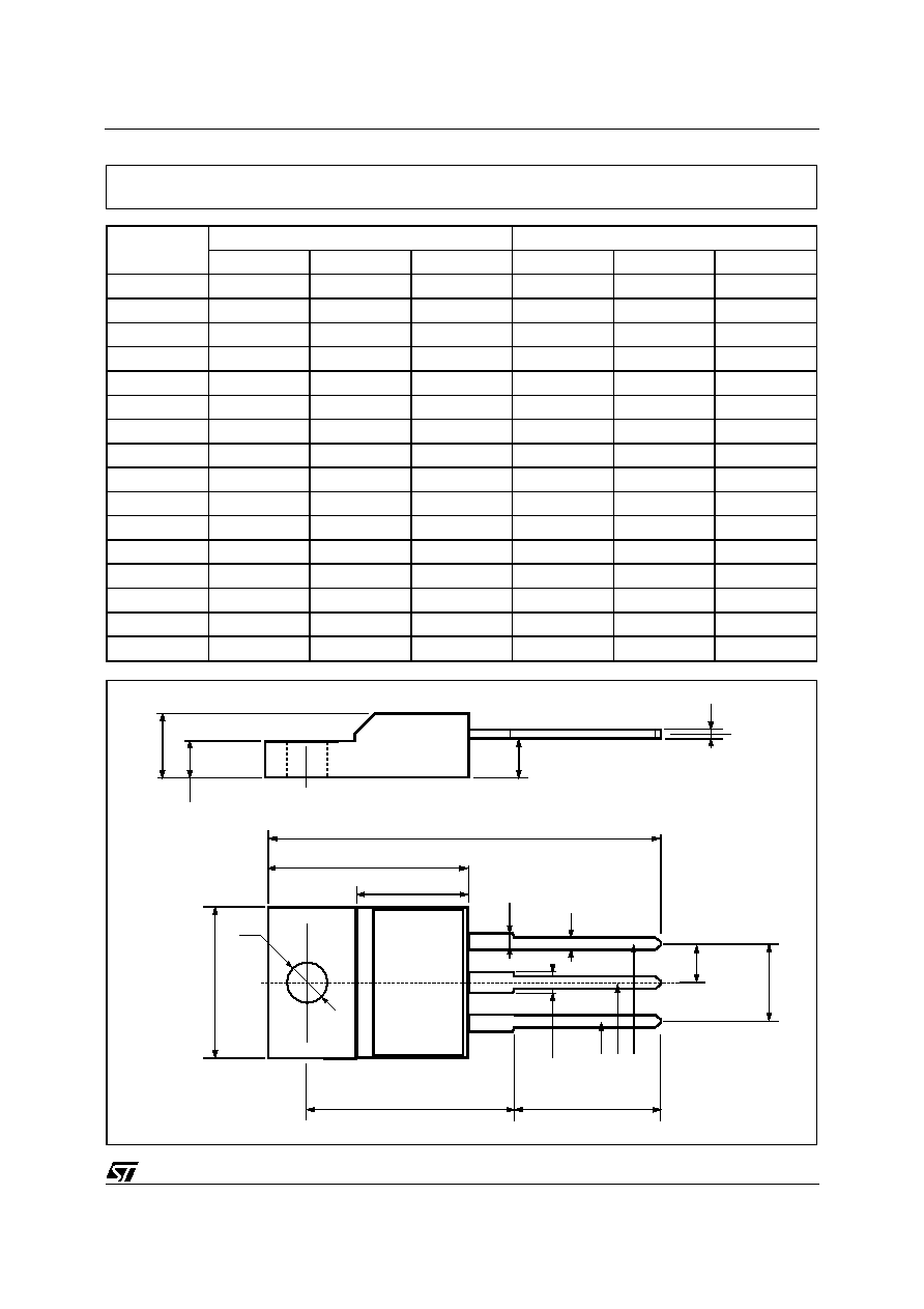
DIM.
mm
inch
MIN.
TYP.
MAX.
MIN.
TYP.
MAX.
A
4.40
4.60
0.173
0.181
C
1.23
1.32
0.048
0.051
D
2.40
2.72
0.094
0.107
D1
1.27
0.050
E
0.49
0.70
0.019
0.027
F
0.61
0.88
0.024
0.034
F1
1.14
1.70
0.044
0.067
F2
1.14
1.70
0.044
0.067
G
4.95
5.15
0.194
0.203
G1
2.4
2.7
0.094
0.106
H2
10.0
10.40
0.393
0.409
L2
16.4
0.645
L4
13.0
14.0
0.511
0.551
L5
2.65
2.95
0.104
0.116
L6
15.25
15.75
0.600
0.620
L7
6.2
6.6
0.244
0.260
L9
3.5
3.93
0.137
0.154
DIA.
3.75
3.85
0.147
0.151
L6
A
C
D
E
D1
F
G
L7
L2
Dia.
F1
L5
L4
H2
L9
F2
G1
TO-220 MECHANICAL DATA
P011C
STP45N10/FI
8/10
DIM.
mm
inch
MIN.
TYP.
MAX.
MIN.
TYP.
MAX.
A
4.4
4.6
0.173
0.181
B
2.5
2.7
0.098
0.106
D
2.5
2.75
0.098
0.108
E
0.4
0.7
0.015
0.027
F
0.75
1
0.030
0.039
F1
1.15
1.7
0.045
0.067
F2
1.15
1.7
0.045
0.067
G
4.95
5.2
0.195
0.204
G1
2.4
2.7
0.094
0.106
H
10
10.4
0.393
0.409
L2
16
0.630
L3
28.6
30.6
1.126
1.204
L4
9.8
10.6
0.385
0.417
L6
15.9
16.4
0.626
0.645
L7
9
9.3
0.354
0.366
ÿ
3
3.2
0.118
0.126
L2
A
B
D
E
H
G
L6
Ø
F
L3
G1
1 2 3
F2
F1
L7
L4
ISOWATT220 MECHANICAL DATA
P011G
STP45N10/FI
9/10

Information furnished is believed to be accurate and reliable. However, STMicroelectronics assumes no responsibility for the consequences
of use of such information nor for any infringement of patents or other rights of third parties which may result from its use. No license is
granted by implication or otherwise under any patent or patent rights of STMicroelectronics. Specification mentioned in this publication are
subject to change without notice. This publication supersedes and replaces all information previously supplied. STMicroelectronics products
are not authorized for use as critical components in life support devices or systems without express written approval of STMicroelectronics.
The ST logo is a trademark of STMicroelectronics
© 1998 STMicroelectronics ≠ Printed in Italy ≠ All Rights Reserved
STMicroelectronics GROUP OF COMPANIES
Australia - Brazil - Canada - China - France - Germany - Italy - Japan - Korea - Malaysia - Malta - Morocco - The Netherlands -
Singapore - Spain - Sweden - Switzerland - Taiwan - Thailand - United Kingdom - U.S.A.
.
STP45N10/FI
10/10