1/11
March 2002
.
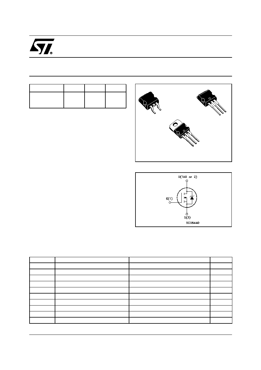
STP55NF03L
STB55NF03L STB55NF03L-1
N-CHANNEL 30V - 0.01
- 55A TO-220/D
2
PAK/I
2
PAK
STripFETTM II POWER MOSFET
s
TYPICAL R
DS
(on) = 0.01
s
OPTIMIZED FOR HIGH SWITCHING
OPERATIONS
s
LOW GATE CHARGE
s
LOGIC LEVEL GATE DRIVE
DESCRIPTION
This Power MOSFET is the latest development of
STMicroelectronis unique "Single Feature SizeTM"
strip-based process. The resulting transistor
shows extremely high packing density for low on-
resistance, rugged avalanche characteristics and
less critical alignment steps therefore a remark-
able manufacturing reproducibility.
APPLICATIONS
s
LOW VOLTAGE DC-DC CONVERTERS
s
HIGH CURRENT, HIGH SWITCHING SPEED
s
HIGH EFFICIENCY SWITCHING CIRCUITS
TYPE
V
DSS
R
DS(on)
I
D
STP55NF03L
STB55NF03L
STB55NF03L-1
30 V
30 V
30 V
<0.013
<0.013
<0.013
55 A
55 A
55 A
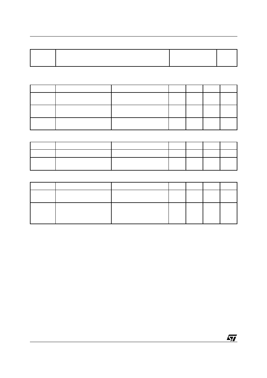
1
2
3
TO-220
1
3
D
2
PAK
TO-263
I
2
PAK
TO-262
1
2
3
INTERNAL SCHEMATIC DIAGRAM
ABSOLUTE MAXIMUM RATINGS
(
∑)
Pulse width limited by safe operating area.
Symbol
Parameter
Value
Unit
V
DS
Drain-source Voltage (V
GS
= 0)
30
V
V
DGR
Drain-gate Voltage (R
GS
= 20 k
)
30
V
V
GS
Gate- source Voltage
± 16
V
I
D
Drain Current (continuous) at T
C
= 25∞C
55
A
I
D
Drain Current (continuous) at T
C
= 100∞C
39
A
I
DM
(
∑)
Drain Current (pulsed)
220
A
P
tot
Total Dissipation at T
C
= 25∞C
80
W
Derating Factor
0.53
W/∞C
T
stg
Storage Temperature
-60 to 175
∞C
T
j
Max. Operating Junction Temperature
175
∞C
STP55NF03L STB55NF03L/-1
2/11
THERMAL DATA
ELECTRICAL CHARACTERISTICS (T
case
= 25 ∞C unless otherwise specified)
OFF
ON
(*)
DYNAMIC
Rthj-case
Rthj-amb
T
l
Thermal Resistance Junction-case
Thermal Resistance Junction-ambient
Maximum Lead Temperature For Soldering Purpose
Max
Max
Typ
1.875
62.5
300
∞C/W
∞C/W
∞C
Symbol
Parameter
Test Conditions
Min.
Typ.
Max.
Unit
V
(BR)DSS
Drain-source
Breakdown Voltage
I
D
= 250 µA, V
GS
= 0
30
V
I
DSS
Zero Gate Voltage
Drain Current (V
GS
= 0)
V
DS
= Max Rating
V
DS
= Max Rating T
C
= 125∞C
1
10
µA
µA
I
GSS
Gate-body Leakage
Current (V
DS
= 0)
V
GS
= ± 16V
±100
nA
Symbol
Parameter
Test Conditions
Min.
Typ.
Max.
Unit
V
GS(th)
Gate Threshold Voltage
V
DS
= V
GS
I
D
= 250 µA
1
V
R
DS(on)
Static Drain-source On
Resistance
V
GS
= 10 V
I
D
= 27.5 A
V
GS
= 4.5 V
I
D
= 27.5 A
0.01
0.013
0.013
0.020
Symbol
Parameter
Test Conditions
Min.
Typ.
Max.
Unit
g
fs (*)
Forward Transconductance
V
DS
> I
D(on)
x R
DS(on)max,
I
D
= 27.5 A
30
S
C
iss
C
oss
C
rss
Input Capacitance
Output Capacitance
Reverse Transfer
Capacitance
V
DS
= 25V, f = 1 MHz, V
GS
= 0
1265
435
115
pF
pF
pF
3/11
STP55NF03L STB55NF03L/-1
SWITCHING ON
SWITCHING OFF
SOURCE DRAIN DIODE
(*)
Pulsed: Pulse duration = 300 µs, duty cycle 1.5 %.
(
∑)
Pulse width limited by safe operating area.
Symbol
Parameter
Test Conditions
Min.
Typ.
Max.
Unit
t
d(on)
t
r
Turn-on Delay Time
Rise Time
V
DD
= 15 V
I
D
= 27.5 A
R
G
= 4.7
V
GS
= 4.5 V
(Resistive Load, Figure 3)
28
400
ns
ns
Q
g
Q
gs
Q
gd
Total Gate Charge
Gate-Source Charge
Gate-Drain Charge
V
DD
= 24 V I
D
= 55 A V
GS
= 4.5V
20
7
10
27
nC
nC
nC
Symbol
Parameter
Test Conditions
Min.
Typ.
Max.
Unit
t
d(off)
t
f
Turn-off Delay Time
Fall Time
V
DD
= 15V
I
D
= 27.5 A
R
G
= 4.7
,
V
GS
= 4.5 V
(Resistive Load, Figure 3)
25
50
ns
ns
Symbol
Parameter
Test Conditions
Min.
Typ.
Max.
Unit
I
SD
I
SDM
(
∑
)
Source-drain Current
Source-drain Current (pulsed)
55
220
A
A
V
SD
(*)
Forward On Voltage
I
SD
= 55 A
V
GS
= 0
1.3
V
t
rr
Q
rr
I
RRM
Reverse Recovery Time
Reverse Recovery Charge
Reverse Recovery Current
I
SD
= 55 A
di/dt = 100A/µs
V
DD
= 30 V
T
j
= 150∞C
(see test circuit, Figure 5)
70
160
4.5
ns
nC
A
ELECTRICAL CHARACTERISTICS (continued)
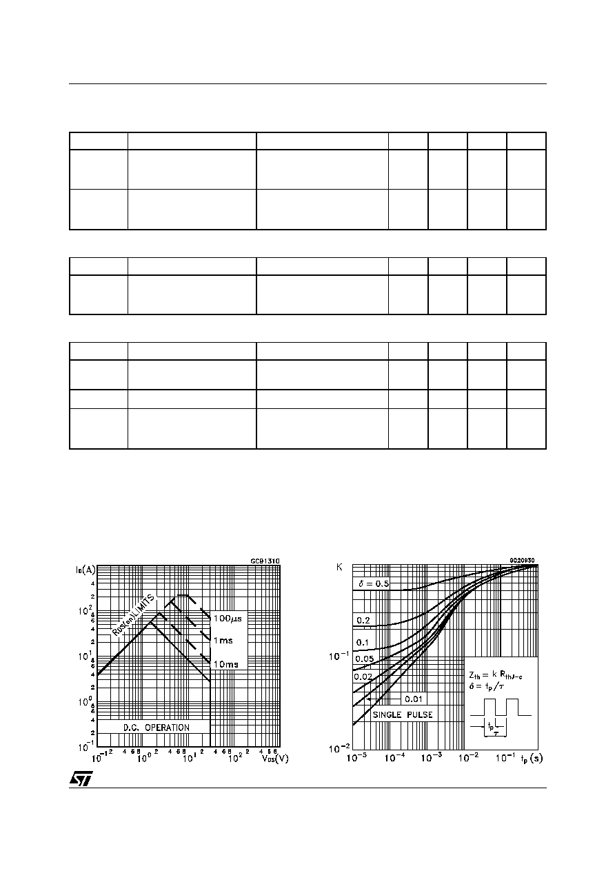
Safe Operating Area
Thermal Impedance
STP55NF03L STB55NF03L/-1
4/11
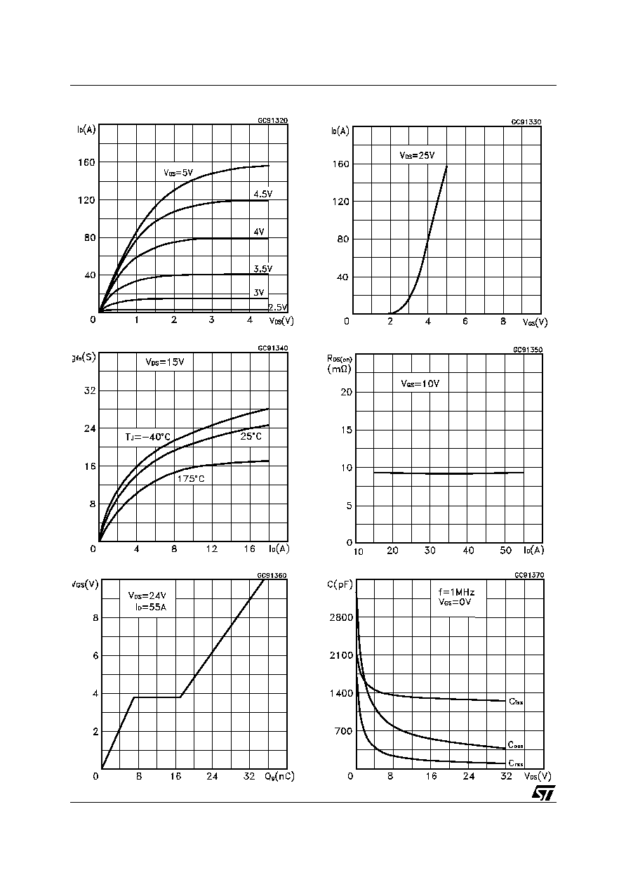
Output Characteristics
Transfer Characteristics
Transconductance
Static Drain-source On Resistance
Gate Charge vs Gate-source Voltage
Capacitance Variations
5/11
STP55NF03L STB55NF03L/-1
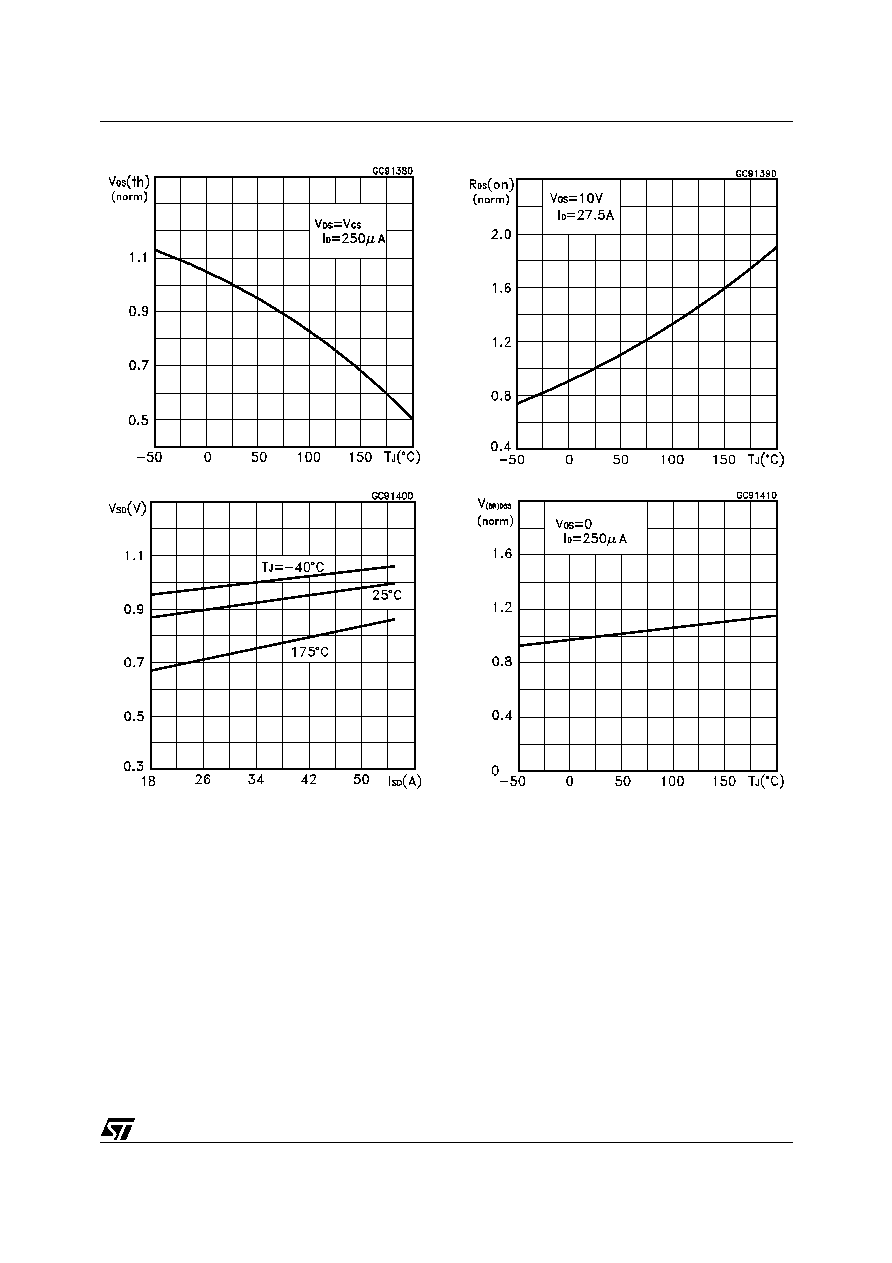
Normalized Gate Threshold Voltage vs Temperature
Normalized
on Resistance vs Temperature
Source-drain Diode Forward Characteristics
Normalized Breakdown Voltage vs Temperature.
.
.
STP55NF03L STB55NF03L/-1
6/11
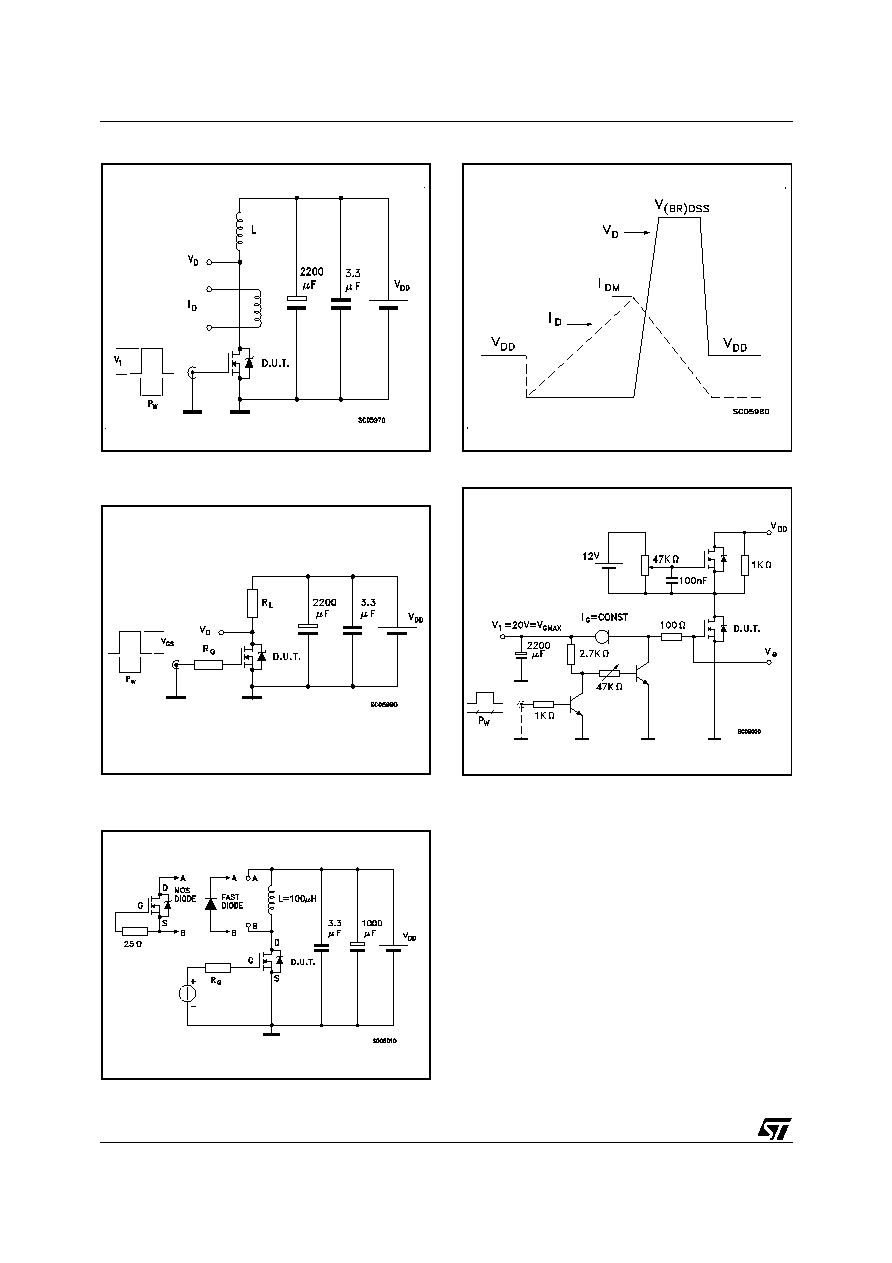
Fig. 1: Unclamped Inductive Load Test Circuit
Fig. 1: Unclamped Inductive Load Test Circuit
Fig. 2: Unclamped Inductive Waveform
Fig. 3: Switching Times Test Circuits For Resistive
Load
Fig. 4: Gate Charge test Circuit
Fig. 5: Test Circuit For Inductive Load Switching
And Diode Recovery Times
7/11
STP55NF03L STB55NF03L/-1
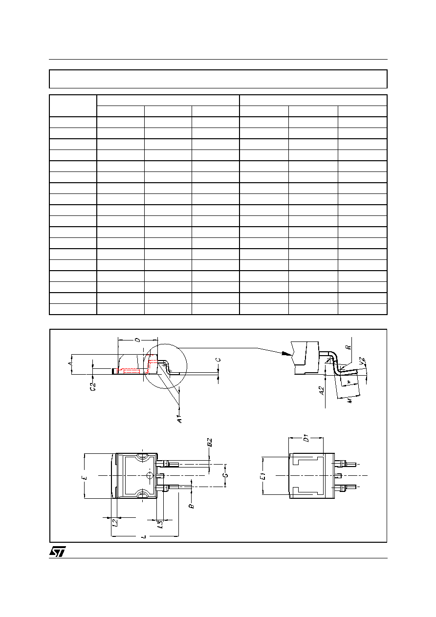
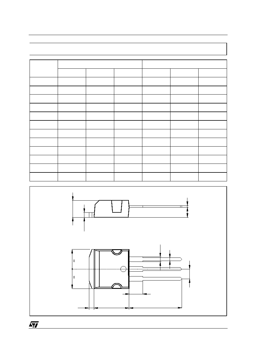
DIM.
mm.
inch.
MIN.
TYP. MAX.
MIN.
TYP. TYP.
A
4.4
4.6
0.173
0.181
A1
2.49
2.69
0.098
0.106
A2
0.03
0.23
0.001
0.009
B
0.7
0.93
0.028
0.037
B2
1.14
1.7
0.045
0.067
C
0.45
0.6
0.018
0.024
C2
1.21
1.36
0.048
0.054
D
8.95
9.35
0.352
0.368
D1
8
0.315
E
10
10.4
0.394
0.409
E1
8.5
0.334
G
4.88
5.28
0.192
0.208
L
15
15.85
0.591
0.624
L2
1.27
1.4
0.050
0.055
L3
1.4
1.75
0.055
0.069
M
2.4
3.2
0.094
0.126
R
0.4
0.016
V2
0∞
4∞
0∞
4∞
D
2
PAK MECHANICAL DATA
STP55NF03L STB55NF03L/-1
8/11
DIM.
mm
inch
MIN.
TYP.
MAX.
MIN.
TYP.
MAX.
A
4.40
4.60
0.173
0.181
C
1.23
1.32
0.048
0.051
D
2.40
2.72
0.094
0.107
D1
1.27
0.050
E
0.49
0.70
0.019
0.027
F
0.61
0.88
0.024
0.034
F1
1.14
1.70
0.044
0.067
F2
1.14
1.70
0.044
0.067
G
4.95
5.15
0.194
0.203
G1
2.4
2.7
0.094
0.106
H2
10.0
10.40
0.393
0.409
L2
16.4
0.645
L4
13.0
14.0
0.511
0.551
L5
2.65
2.95
0.104
0.116
L6
15.25
15.75
0.600
0.620
L7
6.2
6.6
0.244
0.260
L9
3.5
3.93
0.137
0.154
DIA.
3.75
3.85
0.147
0.151
L6
A
C
D
E
D1
F
G
L7
L2
Dia.
F1
L5
L4
H2
L9
F2
G1
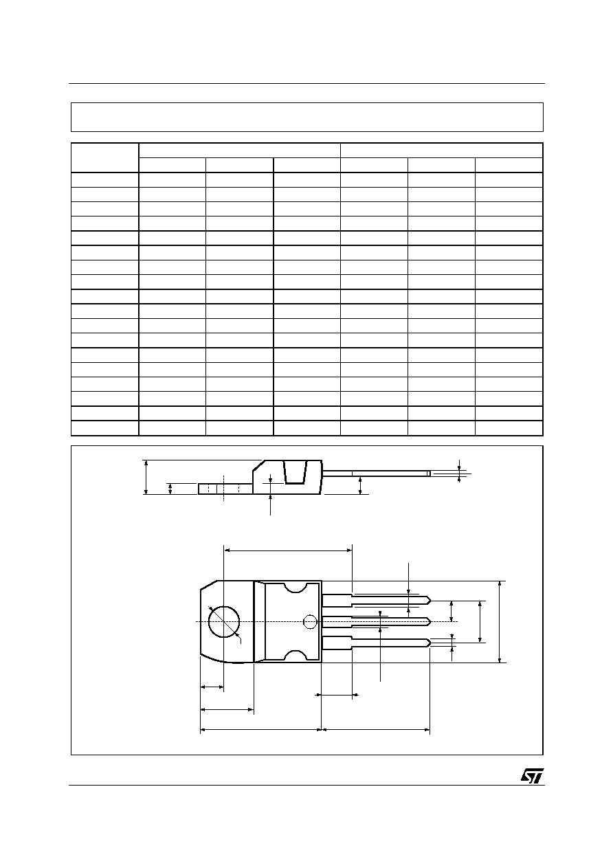
TO-220 MECHANICAL DATA
P011C
9/11
STP55NF03L STB55NF03L/-1
DIM.
mm
inch
MIN.
TYP.
MAX.
MIN.
TYP.
MAX.
A
4.4
4.6
0.173
0.181
A1
2.49
2.69
0.098
0.106
B
0.7
0.93
0.027
0.036
B2
1.14
1.7
0.044
0.067
C
0.45
0.6
0.017
0.023
C2
1.23
1.36
0.048
0.053
D
8.95
9.35
0.352
0.368
e
2.4
2.7
0.094
0.106
E
10
10.4
0.393
0.409
L
13.1
13.6
0.515
0.531
L1
3.48
3.78
0.137
0.149
L2
1.27
1.4
0.050
0.055
L
L1
B2
B
D
E
A
C2
C
A1
L2
e
P011P5/E
TO-262 (I
2
PAK) MECHANICAL DATA
STP55NF03L STB55NF03L/-1
10/11
DIM.
mm
inch
MIN.
MAX.
MIN.
MAX.
A0
10.5
10.7
0.413
0.421
B0
15.7
15.9
0.618
0.626
D
1.5
1.6
0.059
0.063
D1
1.59
1.61
0.062
0.063
E
1.65
1.85
0.065
0.073
F
11.4
11.6
0.449
0.456
K0
4.8
5.0
0.189
0.197
P0
3.9
4.1
0.153
0.161
P1
11.9
12.1
0.468
0.476
P2
1.9
2.1
0075
0.082
R
50
1.574
T
0.25
0.35
.0.0098
0.0137
W
23.7
24.3
0.933
0.956
DIM.
mm
inch
MIN.
MAX.
MIN.
MAX.
A
330
12.992
B
1.5
0.059
C
12.8
13.2
0.504
0.520
D
20.2
0.795
G
24.4
26.4
0.960
1.039
N
100
3.937
T
30.4
1.197
BASE QTY
BULK QTY
1000
1000
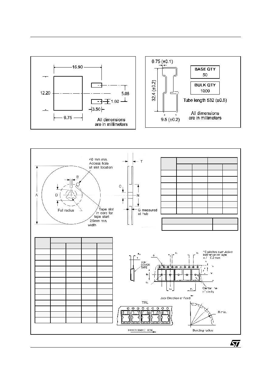
REEL MECHANICAL DATA
* on sales type
TUBE SHIPMENT (no suffix)*
TAPE AND REEL SHIPMENT (suffix "T4")*
D
2
PAK FOOTPRINT
TAPE MECHANICAL DATA

11/11
STP55NF03L STB55NF03L/-1
Information furnished is believed to be accurate and reliable. However, STMicroelectronics assumes no responsibility for the consequences
of use of such information nor for any infringement of patents or other rights of third parties which may result from its use. No license is granted
by implication or otherwise under any patent or patent rights of STMicroelectronics. Specifications mentioned in this publication are subject
to change without notice. This publication supersedes and replaces all information previously supplied. STMicroelectronics products are not
authorized for use as critical components in life support devices or systems without express written approval of STMicroelectronics.
The ST logo is registered trademark of STMicroelectronics
Æ
2002 STMicroelectronics - All Rights Reserved
All other names are the property of their respective owners.
STMicroelectronics GROUP OF COMPANIES
Australia - Brazil - Canada - China - Finland - France - Germany - Hong Kong - India - Israel - Italy - Japan - Malaysia - Malta - Morocco -
Singapore - Spain - Sweden - Switzerland - United Kingdom - United States.
http://www.st.com