STP60NE10
STP60NE10FP
N - CHANNEL 100V - 0.016
- 60A TO-220/TO-220FP
STripFET
TM
POWER MOSFET
s
TYPICAL R
DS(on)
= 0.016
s
EXCEPTIONAL dv/dt CAPABILITY
s
100% AVALANCHE TESTED
s
APPLICATION ORIENTED
CHARACTERIZATION
DESCRIPTION
This Power MOSFET is the latest development of
STMicroelectronics
unique
"Single
Feature
Size
TM
" strip-based process. The resulting transi-
stor shows extremely high packing density for low
on-resistance, rugged avalanche characteristics
and less critical alignment steps therefore a re-
markable manufacturing reproducibility.
APPLICATIONS
s
SOLENOID AND RELAY DRIVERS
s
MOTOR CONTROL, AUDIO AMPLIFIERS
s
DC-DC CONVERTERS
s
AUTOMOTIVE ENVIRONMENT (INJECTION,
ABS, AIR-BAG, LAMPDRIVERS, Etc.)
Æ
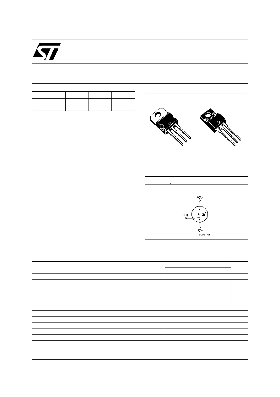
INTERNAL SCHEMATIC DIAGRAM
ABSOLUTE MAXIMUM RATINGS
Symbol
Parameter
Value
Un it
STP60NE10
STP60NE10FP
V
DS
Drain-source Volt age (V
GS
= 0)
100
V
V
DGR
Drain- gat e Voltage (R
G S
= 20 k
)
100
V
V
GS
Gat e-source Voltage
±
20
V
I
D
Drain Current (continuous) at T
c
= 25
o
C
60
30
A
I
D
Drain Current (continuous) at T
c
= 100
o
C
42
21
A
I
DM
(
∑
)
Drain Current (pulsed)
240
120
A
P
tot
Tot al Dissipation at T
c
= 25
o
C
160
50
W
Derating F act or
1.06
0.37
W /
o
C
V
ISO
Insulation Withstand Voltage (DC)
2000
V
dv/dt
Peak Diode Recovery voltage slope
7
V/ns
T
s tg
Storage Temperature
-65 to 175
o
C
T
j
Max. Operating Junction Temperature
175
o
C
(
∑
) Pulse width limited by safe operating area
(
1
) I
SD
60 A, di/dt
300 A/
µ
s, V
DD
V
(BR)DSS
, T
j
T
JMAX
TYPE
V
DSS
R
DS(on)
I
D
STP60NE10
STP60NE10FP
100 V
100 V
< 0.022
< 0.022
60 A
30 A
May 1999
TO-220
TO-220FP
1
2
3
1
2
3
1/9
THERMAL DATA
TO-220
TO-220FP
R
thj -case
Thermal Resistance Junction-case
Max
0. 94
2.7
o
C/W
R
thj -amb
R
thc-sink
T
l
Thermal Resistance Junction-ambient
Max
Thermal Resistance Case-sink
Typ
Maximum Lead Temperature F or Soldering Purpose
62.5
0.5
300
o
C/W
o
C/W
o
C
AVALANCHE CHARACTERISTICS
Symbo l
Parameter
Max Value
Unit
I
AR
Avalanche Current, Repetitive or Not-Repetitive
(pulse width limited by T
j
max)
60
A
E
AS
Single Pulse Avalanche Energy
(starting T
j
= 25
o
C, I
D
= I
AR
, V
DD
= 35V)
100
mJ
ELECTRICAL CHARACTERISTICS (T
case
= 25
o
C unless otherwise specified)
OFF
Symbo l
Parameter
Test Con ditions
Min.
Typ.
Max.
Unit
V
(BR)DSS
Drain-source
Breakdown Voltage
I
D
= 250
µ
A
V
GS
= 0
100
V
I
DSS
Zero Gat e Voltage
Drain Current (V
GS
= 0)
V
DS
= Max Rat ing
V
DS
= Max Rat ing
T
c
= 125
o
C
1
10
µ
A
µ
A
I
G SS
Gat e-body Leakage
Current (V
DS
= 0)
V
GS
=
±
20 V
±
100
nA
ON (
)
Symbo l
Parameter
Test Con ditions
Min.
Typ.
Max.
Unit
V
G S(th)
Gat e Threshold Voltage V
DS
= V
GS
I
D
= 250
µ
A
2
3
4
V
R
DS(on)
Static Drain-source On
Resistance
V
GS
= 10V
I
D
= 30 A
0.016
0.022
I
D(o n)
On State Drain Current
V
DS
> I
D(o n)
x R
DS(on )ma x
V
GS
= 10 V
60
A
DYNAMIC
Symbo l
Parameter
Test Con ditions
Min.
Typ.
Max.
Unit
g
f s
(
)
Forward
Transconductance
V
DS
> I
D(o n)
x R
DS(on )ma x
I
D
=18 A
30
S
C
iss
C
os s
C
rss
Input Capacitance
Out put Capacitance
Reverse Transfer
Capacitance
V
DS
= 25 V
f = 1 MHz
V
GS
= 0
5300
640
215
pF
pF
pF
STP60NE10/FP
2/9
ELECTRICAL CHARACTERISTICS (continued)
SWITCHING ON
Symbo l
Parameter
Test Con ditions
Min.
Typ.
Max.
Unit
t
d(on)
t
r
Turn-on Delay T ime
Rise Time
V
DD
= 50 V
I
D
= 30 A
R
G
= 4.7
V
G S
= 10 V
(Resistive Load, see fig. 3)
28
100
ns
ns
Q
g
Q
gs
Q
gd
Tot al G ate Charge
Gat e-Source Charge
Gat e-Drain Charge
V
DD
= 80 V I
D
= 60 A V
GS
= 10 V
142
27
59
185
nC
nC
nC
SWITCHING OFF
Symbo l
Parameter
Test Con ditions
Min.
Typ.
Max.
Unit
t
d(of f)
t
f
Turn-off Delay T ime
Fall T ime
V
DD
= 50 V
I
D
= 30 A
R
G
= 4.7
V
G S
= 10 V
(Resistive Load, see fig. 3)
160
45
ns
ns
t
r (Voff)
t
f
t
c
Off -volt age Rise T ime
Fall T ime
Cross-over Time
V
clamp
= 80 V
I
D
= 60 A
R
G
=
4.7
V
GS
= 10 V
(Induct ive Load, see fig. 5)
40
45
85
ns
ns
ns
SOURCE DRAIN DIODE
Symbo l
Parameter
Test Con ditions
Min.
Typ.
Max.
Unit
I
SD
I
SDM
(
∑
)
Source-drain Current
Source-drain Current
(pulsed)
60
240
A
A
V
SD
(
)
Forward On Voltage
I
SD
= 60 A
V
GS
= 0
1. 5
V
t
rr
Q
rr
I
RRM
Reverse Recovery
Time
Reverse Recovery
Charge
Reverse Recovery
Current
I
SD
= 60 A
di/dt = 100 A/
µ
s
V
DD
= 50 V
T
j
= 150
o
C
(see t est circuit, f ig. 5)
170
1.02
12
ns
µ
C
A
(
) Pulsed: Pulse duration = 300
µ
s, duty cycle 1.5 %
(
∑
) Pulse width limited by safe operating area
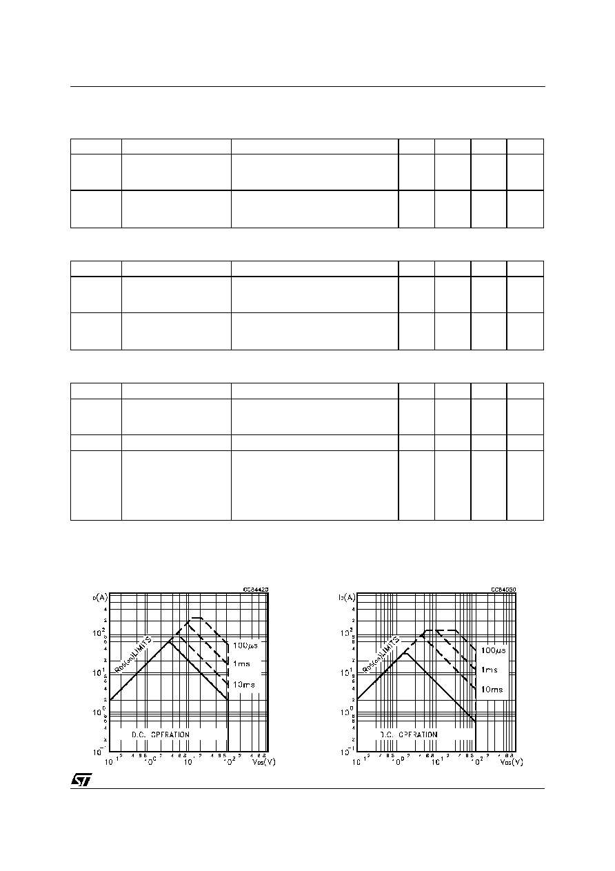
Safe Operating Area for TO-220
Safe Operating Area for TO-220FP
STP60NE10/FP
3/9
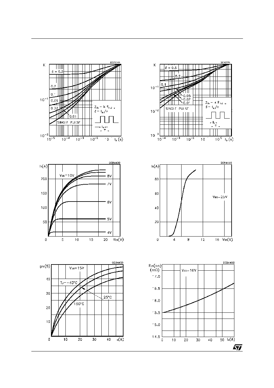
Thermal Impedance for TO-220
Output Characteristics
Transconductance
Thermal Impedance forTO-220FP
Transfer Characteristics
Static Drain-source On Resistance
STP60NE10/FP
4/9
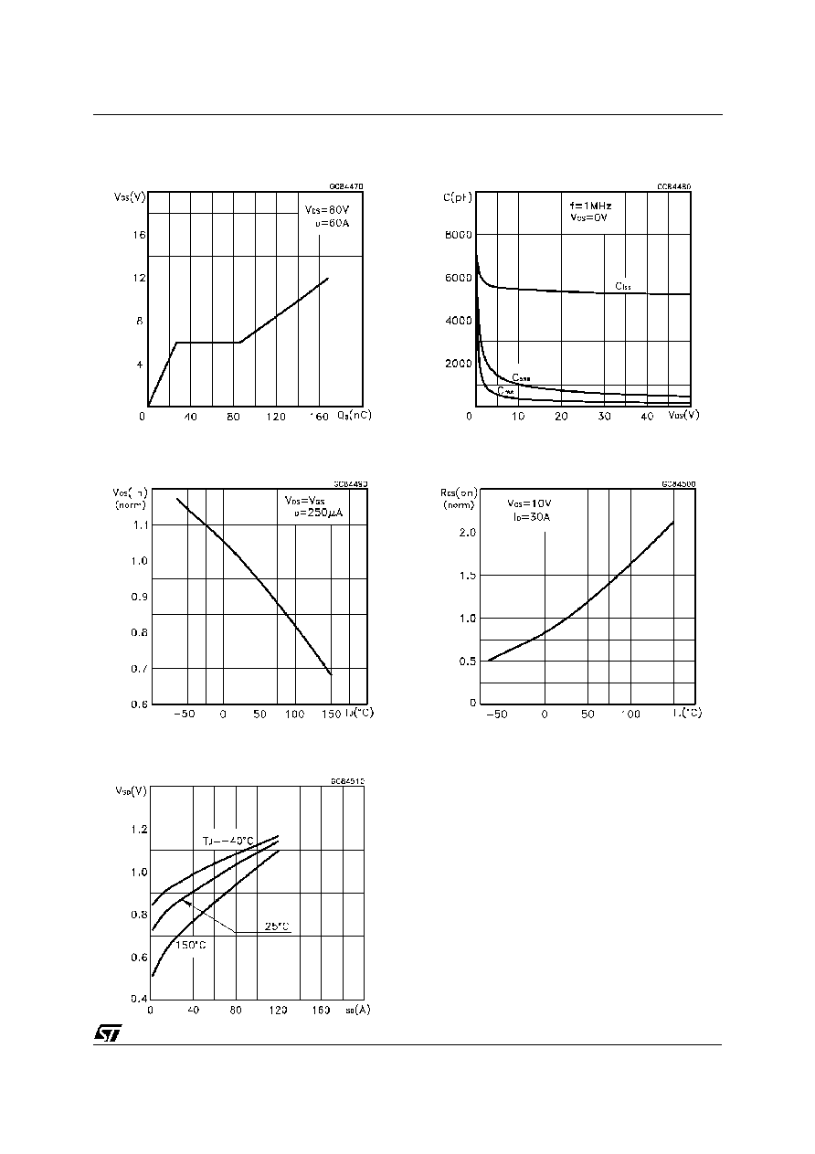
Gate Charge vs Gate-source Voltage
Normalized Gate Threshold Voltage vs
Temperature
Source-drain Diode Forward Characteristics
Capacitance Variations
Normalized On Resistance vs Temperature
STP60NE10/FP
5/9
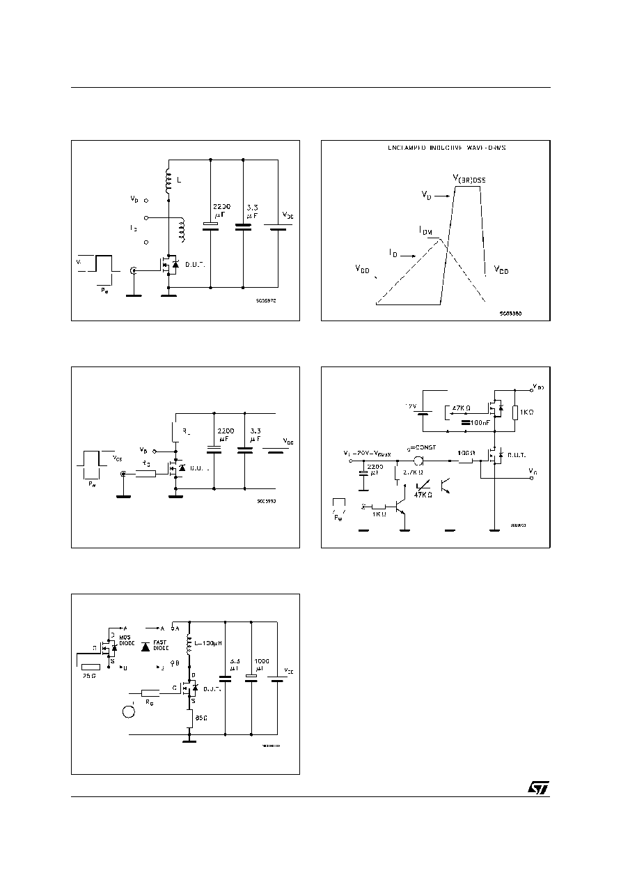
Fig. 1: Unclamped Inductive Load Test Circuit
Fig. 3: Switching Times Test Circuits For
Resistive Load
Fig. 2: Unclamped Inductive Waveform
Fig. 4: Gate Charge test Circuit
Fig. 5: Test Circuit For Inductive Load Switching
And Diode Recovery Times
STP60NE10/FP
6/9
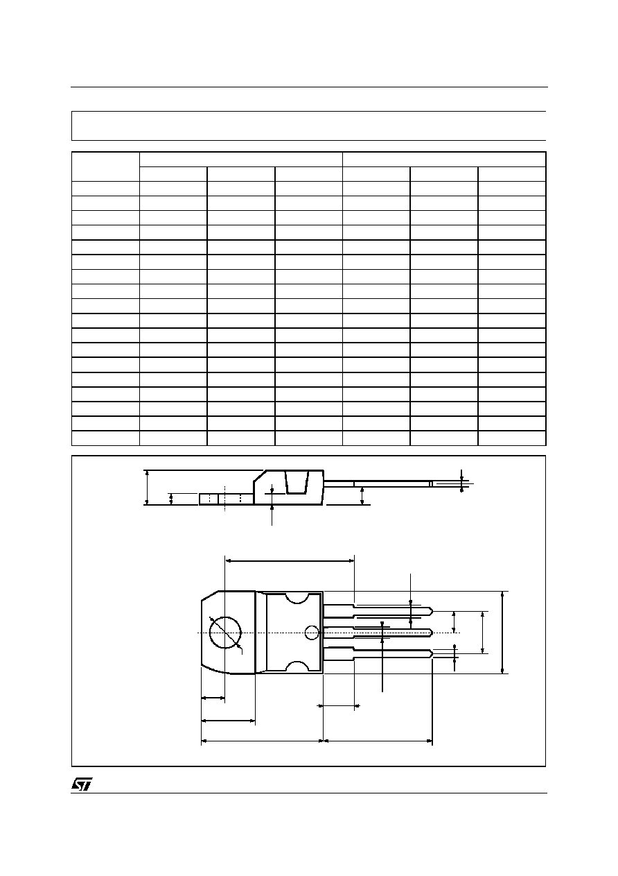
DIM.
mm
inch
MIN.
TYP.
MAX.
MIN.
TYP.
MAX.
A
4.40
4.60
0.173
0.181
C
1.23
1.32
0.048
0.051
D
2.40
2.72
0.094
0.107
D1
1.27
0.050
E
0.49
0.70
0.019
0.027
F
0.61
0.88
0.024
0.034
F1
1.14
1.70
0.044
0.067
F2
1.14
1.70
0.044
0.067
G
4.95
5.15
0.194
0.203
G1
2.4
2.7
0.094
0.106
H2
10.0
10.40
0.393
0.409
L2
16.4
0.645
L4
13.0
14.0
0.511
0.551
L5
2.65
2.95
0.104
0.116
L6
15.25
15.75
0.600
0.620
L7
6.2
6.6
0.244
0.260
L9
3.5
3.93
0.137
0.154
DIA.
3.75
3.85
0.147
0.151
L6
A
C
D
E
D1
F
G
L7
L2
Dia.
F1
L5
L4
H2
L9
F2
G1
TO-220 MECHANICAL DATA
P011C
STP60NE10/FP
7/9
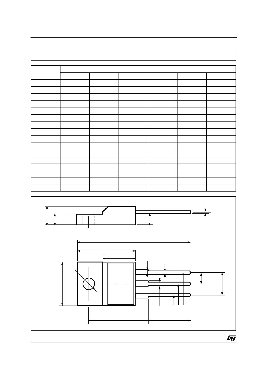
DIM.
mm
inch
MIN.
TYP.
MAX.
MIN.
TYP.
MAX.
A
4.4
4.6
0.173
0.181
B
2.5
2.7
0.098
0.106
D
2.5
2.75
0.098
0.108
E
0.45
0.7
0.017
0.027
F
0.75
1
0.030
0.039
F1
1.15
1.7
0.045
0.067
F2
1.15
1.7
0.045
0.067
G
4.95
5.2
0.195
0.204
G1
2.4
2.7
0.094
0.106
H
10
10.4
0.393
0.409
L2
16
0.630
L3
28.6
30.6
1.126
1.204
L4
9.8
10.6
0.385
0.417
L6
15.9
16.4
0.626
0.645
L7
9
9.3
0.354
0.366
ÿ
3
3.2
0.118
0.126
L2
A
B
D
E
H
G
L6
Ø
F
L3
G1
1 2 3
F2
F1
L7
L4
TO-220FP MECHANICAL DATA
STP60NE10/FP
8/9

Information furnished is believ ed to be accurate and reliable. However, STMicroelectronics assumes no responsibil ity for the consequences
of use of such information nor for any infringement of patents or other rights of third parties which may result from its use. No license is
granted by implication or otherwise under any patent or patent rights of STMicroelectronics. Specific ation mentioned in this publication are
subjec t to change without notice. This publication supersedes and replaces all information previously supplied. STMicroelectronics products
are not authorized for use as critical components in life support devices or systems without express written approval of STMicroelectronics.
The ST logo is a trademark of STMicroelectronics
©
1999 STMicroelectronics ≠ Printed in Italy ≠ All Rights Reserved
STMicroelectronics GROUP OF COMPANIES
Australia - Brazil - Canada - China - France - Germany - Italy - Japan - Korea - Malaysia - Malta - Mexico - Morocco - The Netherlands -
Singapore - Spain - Sweden - Switzerland - Taiwan - Thailand - United Kingdom - U.S.A.
http://www.st.com
.
STP60NE10/FP
9/9