1/8
November 2002
STP60NS04ZB
N-CHANNEL CLAMPED 10m
- 60A TO-220
FULLY PROTECTED MESH OVERLAYTM MOSFET
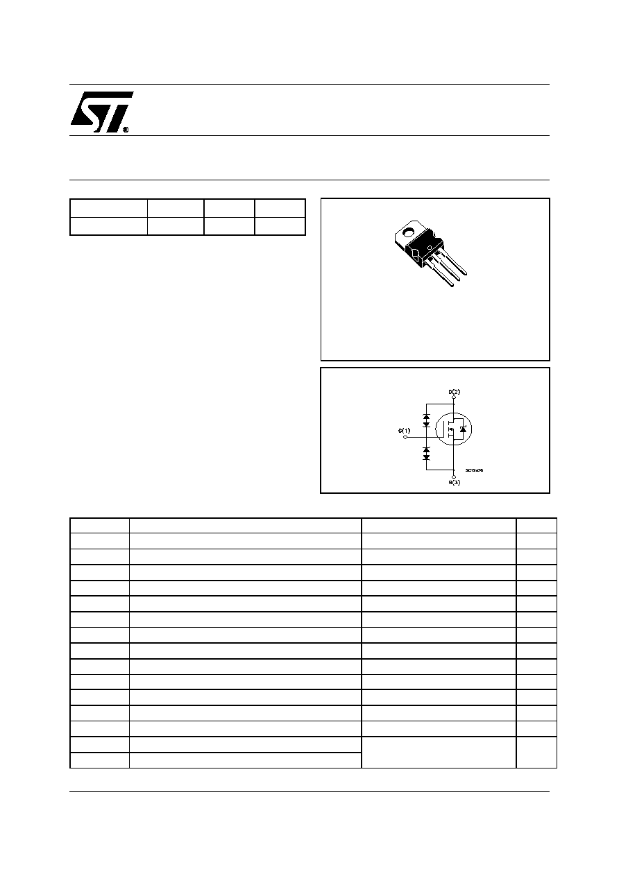
TO-220
1
2
3
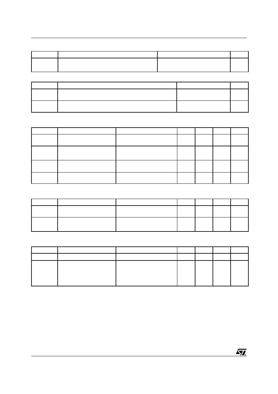
INTERNAL SCHEMATIC DIAGRAM
s
TYPICAL R
DS
(on) = 0.010
s
100% AVALANCHE TESTED
s
LOW CAPACITANCE AND GATE CHARGE
s
175∞C MAXIMUM JUNCTION TEMPERATURE
DESCRIPTION
This fully clamped MOSFET is produced by using
the latest advanced Company's Mesh Overlay pro-
cess which is based on a novel strip layout. The in-
herent benefits of the new technology coupled with
the extra clamping capabilities make this product
particularly suitable for the harshest operation con-
ditions such as those encountered in the automotive
environment .Any other application requiring extra
ruggedness is also recommended.
APPLICATIONS
s
ABS,SOLENOID DRIVERS
s
MOTOR CONTROL
s
DC-DC CONVERTERS
ABSOLUTE MAXIMUM RATINGS
(∑)Pulse width limited by safe operating area
TYPE
V
DSS
R
DS(on)
I
D
STP60NS04ZB
CLAMPED
< 0.015
60 A
Symbol
Parameter
Value
Unit
V
DS
Drain-source Voltage (V
GS
= 0)
CLAMPED
V
V
DG
Drain-gate Voltage
CLAMPED
V
V
GS
Gate- source Voltage
CLAMPED
V
I
D
Drain Current (continuous) at T
C
= 25∞C
60
A
I
D
Drain Current (continuous) at T
C
= 100∞C
42
A
I
DG
Drain Gate Current (continuous)
±
50
mA
I
GS
Gate Source Current (continuous)
±
50
mA
I
DM
( )
Drain Current (pulsed)
240
A
P
TOT
Total Dissipation at T
C
= 25∞C
150
W
Derating Factor
1
W/∞C
V
ESD(G-S)
Gate-Source ESD(HBM-C=100 pF, R=1.5 K
)
6
kV
V
ESD(G-D)
Gate-Drain ESD(HBM-C=100 pF, R=1.5 K
)
4
kV
V
ESD(D-S)
Drain-Source ESD(HBM-C=100 pF, R=1.5 K
)
4
kV
T
stg
Storage Temperature
≠65 to 175
∞C
T
j
Max. Operating Junction Temperature
STP60NS04ZB
2/8
THERMAL DATA
AVALANCHE CHARACTERISTICS
ELECTRICAL CHARACTERISTICS (T
CASE
= 25∞C UNLESS OTHERWISE SPECIFIED)
OFF
ON (1)
DYNAMIC
Rthj-case
Thermal Resistance Junction-case Max
1.0
∞C/W
Rthj-amb
Thermal Resistance Junction-ambient Max
62.5
∞C/W
T
l
Maximum Lead Temperature For Soldering Purpose
300
∞C
Symbol
Parameter
Max Value
Unit
I
AR
Avalanche Current, Repetitive or Not-Repetitive
(pulse width limited by T
j
max,
< 1%)
60
A
E
AS
Single Pulse Avalanche Energy
(starting T
j
= 25 ∞C, I
D
= I
AR
, V
DD
= 30 V )
400
mJ
Symbol
Parameter
Test Conditions
Min.
Typ.
Max.
Unit
V
(BR)DSS
Clamped Voltage
I
D
= 1 mA, V
GS
= 0
-40 < Tj < 175 ∞C
33
V
I
DSS
Zero Gate Voltage
Drain Current (V
GS
= 0)
V
DS
= 16 V,T
j
= 150 ∞C
50
µA
V
DS
= 16 V,T
j
= 175 ∞C
100
µA
I
GSS
Gate-body Leakage
Current (V
DS
= 0)
V
GS
= ±10 V,T
j
= 175 ∞C
V
GS
= ±16 V,T
j
= 175 ∞C
50
150
µA
µA
V
GSS
Gate-Source
Breakdown Voltage
I
GS
= ±100 µA
18
V
Symbol
Parameter
Test Conditions
Min.
Typ.
Max.
Unit
V
GS(th)
Gate Threshold Voltage
V
DS
= V
GS
, I
D
= 1 mA
-40 < Tj < 150 ∞C
1.7
3
4.2
V
R
DS(on)
Static Drain-source On
Resistance
V
GS
= 10 V, I
D
= 30 A
11
15
m
V
GS
= 16 V, I
D
= 30 A
10
14
m
Symbol
Parameter
Test Conditions
Min.
Typ.
Max.
Unit
g
fs
(1)
Forward Transconductance
V
DS
=15 V ,I
D
= 30 A
20
40
S
C
iss
Input Capacitance
V
DS
= 25 V, f = 1 MHz, V
GS
= 0
1700
2100
pF
C
oss
Output Capacitance
800
1000
pF
C
rss
Reverse Transfer
Capacitance
190
240
pF
3/8
STP60NS04ZB
ELECTRICAL CHARACTERISTICS (CONTINUED)
SWITCHING ON
SWITCHING OFF
SOURCE DRAIN DIODE
Note: 1. Pulsed: Pulse duration = 300 µs, duty cycle 1.5 %.
2. Pulse width limited by safe operating area.
Symbol
Parameter
Test Conditions
Min.
Typ.
Max.
Unit
Q
g
Total Gate Charge
V
DD
= 18 V, I
D
= 60 A,
V
GS
= 10 V
48
62
nC
Q
gs
Gate-Source Charge
13
nC
Q
gd
Gate-Drain Charge
16
nC
Symbol
Parameter
Test Conditions
Min.
Typ.
Max.
Unit
t
r(Voff)
t
f
t
c
Off Voltage Rise Time
Fall Time
Cross-over Time
V
CLAMP
= 30 V, I
D
= 60 A,
R
G
= 4.7
,
V
GS
= 10 V
(see test circuit, Figure 3)
60
45
100
75
60
130
ns
ns
ns
Symbol
Parameter
Test Conditions
Min.
Typ.
Max.
Unit
I
SD
Source-drain Current
60
A
I
SDM
(2)
Source-drain Current (pulsed)
240
A
V
SD
(1)
Forward On Voltage
I
SD
= 60 A, V
GS
= 0
1.5
V
t
rr
Reverse Recovery Time
I
SD
= 60 A, di/dt = 100 A/µs
V
DD
= 15 V, T
j
= 150∞C
(see test circuit, Figure 5)
50
ns
Q
rr
Reverse Recovery Charge
62
nC
I
RRM
Reverse Recovery Current
2.6
A
Thermal Impedance
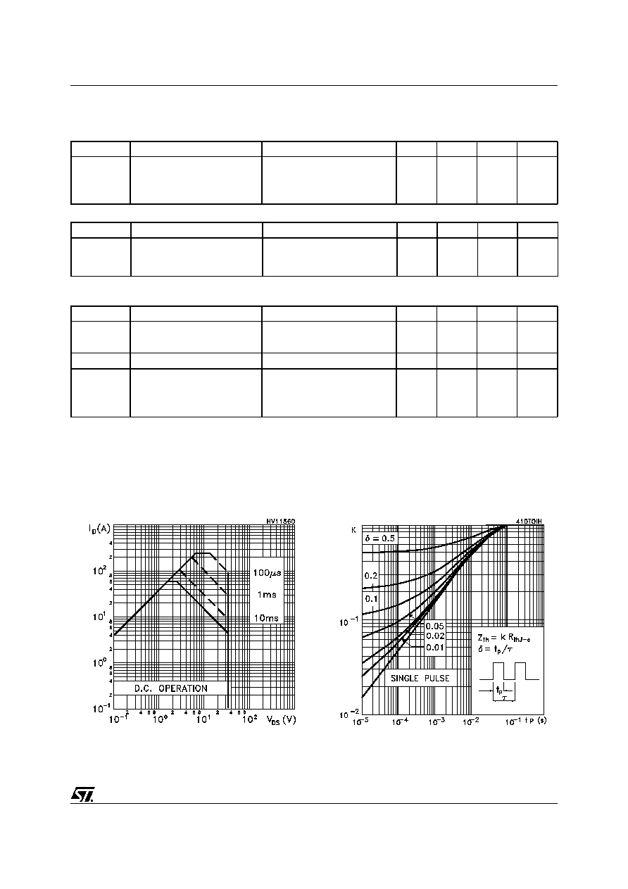
Safe Operating Area
STP60NS04ZB
4/8
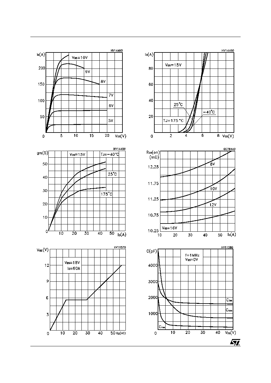
Transfer Characteristics
Transconductance
Output Characteristics
Gate Charge vs Gate-source Voltage
Capacitance Variations
Static Drain-source On Resistance
5/8
STP60NS04ZB
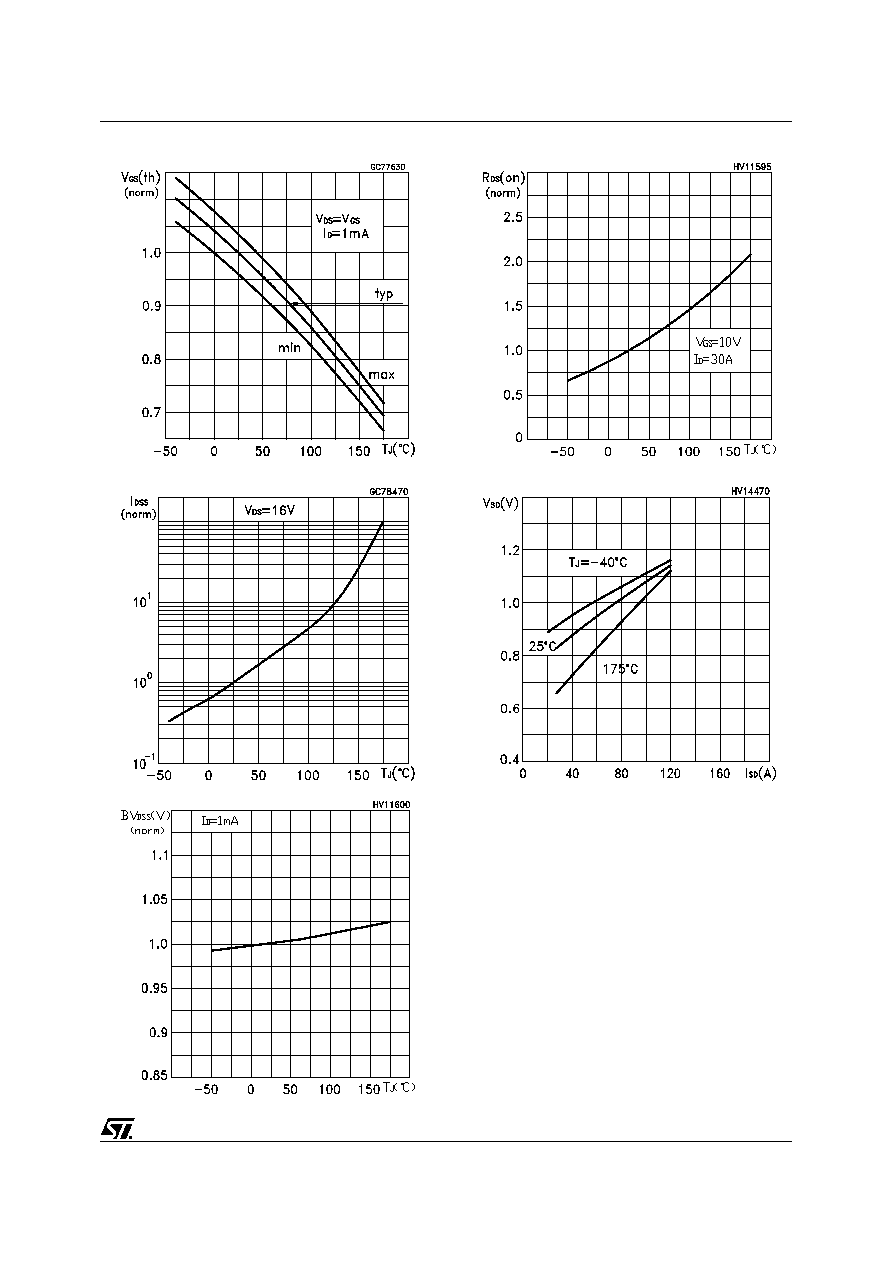
Normalized On Resistance vs Temperature
Source-drain Diode Forward Characteristics
Normalized Gate Thereshold Voltage vs Temp.
Zero Gate Voltage Drain Current vs Temperature
Normalized BVDSS vs Temperature
STP60NS04ZB
6/8
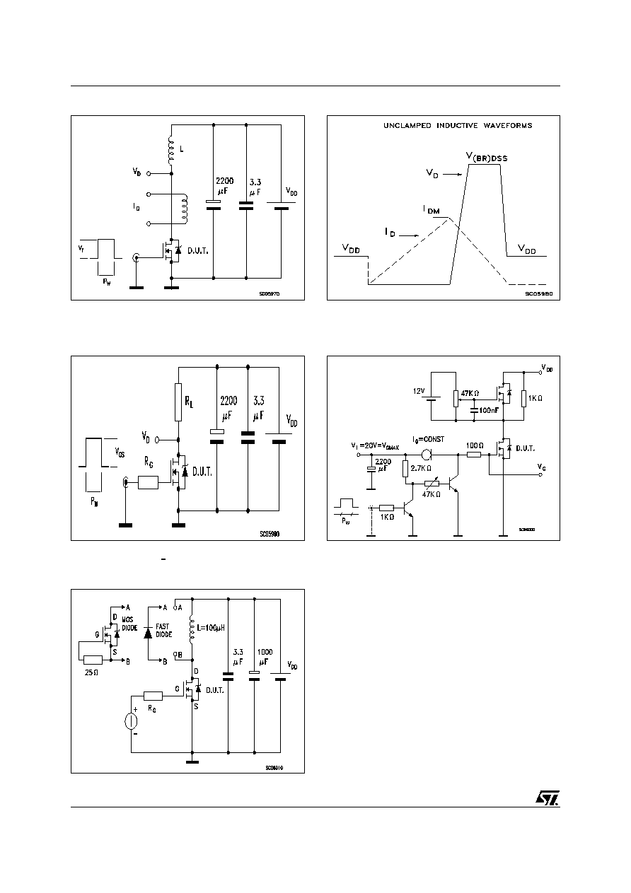
Fig. 5: Test Circuit For Inductive Load Switching
And Diode Recovery Times
Fig. 4: Gate Charge test Circuit
Fig. 2: Unclamped Inductive Waveform
Fig. 1: Unclamped Inductive Load Test Circuit
Fig. 3: Switching Times Test Circuit For
Resistive Load
7/8
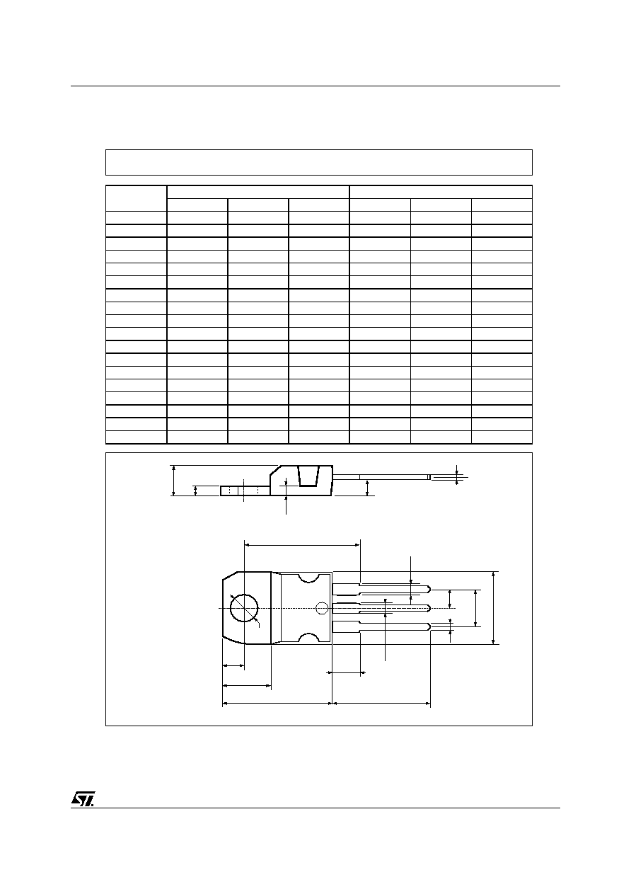
STP60NS04ZB
DIM.
mm
inch
MIN.
TYP.
MAX.
MIN.
TYP.
MAX.
A
4.40
4.60
0.173
0.181
C
1.23
1.32
0.048
0.051
D
2.40
2.72
0.094
0.107
D1
1.27
0.050
E
0.49
0.70
0.019
0.027
F
0.61
0.88
0.024
0.034
F1
1.14
1.70
0.044
0.067
F2
1.14
1.70
0.044
0.067
G
4.95
5.15
0.194
0.203
G1
2.4
2.7
0.094
0.106
H2
10.0
10.40
0.393
0.409
L2
16.4
0.645
L4
13.0
14.0
0.511
0.551
L5
2.65
2.95
0.104
0.116
L6
15.25
15.75
0.600
0.620
L7
6.2
6.6
0.244
0.260
L9
3.5
3.93
0.137
0.154
DIA.
3.75
3.85
0.147
0.151
L6
A
C
D
E
D1
F
G
L7
L2
Dia.
F1
L5
L4
H2
L9
F2
G1
TO-220 MECHANICAL DATA
P011C

STP60NS04ZB
8/8
Information furnished is believed to be accurate and reliable. However, STMicroelectronics assumes no responsibility for the
consequences of use of such information nor for any infringement of patents or other rights of third parties which may result from
its use. No license is granted by implication or otherwise under any patent or patent rights of STMicroelectronics. Specifications
mentioned in this publication are subject to change without notice. This publication supersedes and replaces all information
previously supplied. STMicroelectronics products are not authorized for use as critical components in life support devices or
systems without express written approval of STMicroelectronics.
© The ST logo is a registered trademark of STMicroelectronics
© 2002 STMicroelectronics - Printed in Italy - All Rights Reserved
STMicroelectronics GROUP OF COMPANIES
Australia - Brazil - Canada - China - Finland - France - Germany - Hong Kong - India - Israel - Italy - Japan - Malaysia - Malta - Morocco
Singapore - Spain - Sweden - Switzerland - United Kingdom - United States.
© http://www.st.com