1/8
March 2004
.
STP62NS04Z
N-CHANNEL CLAMPED 12.5m
- 62A TO-220
FULLY PROTECTED MESH OVERLAYTM MOSFET
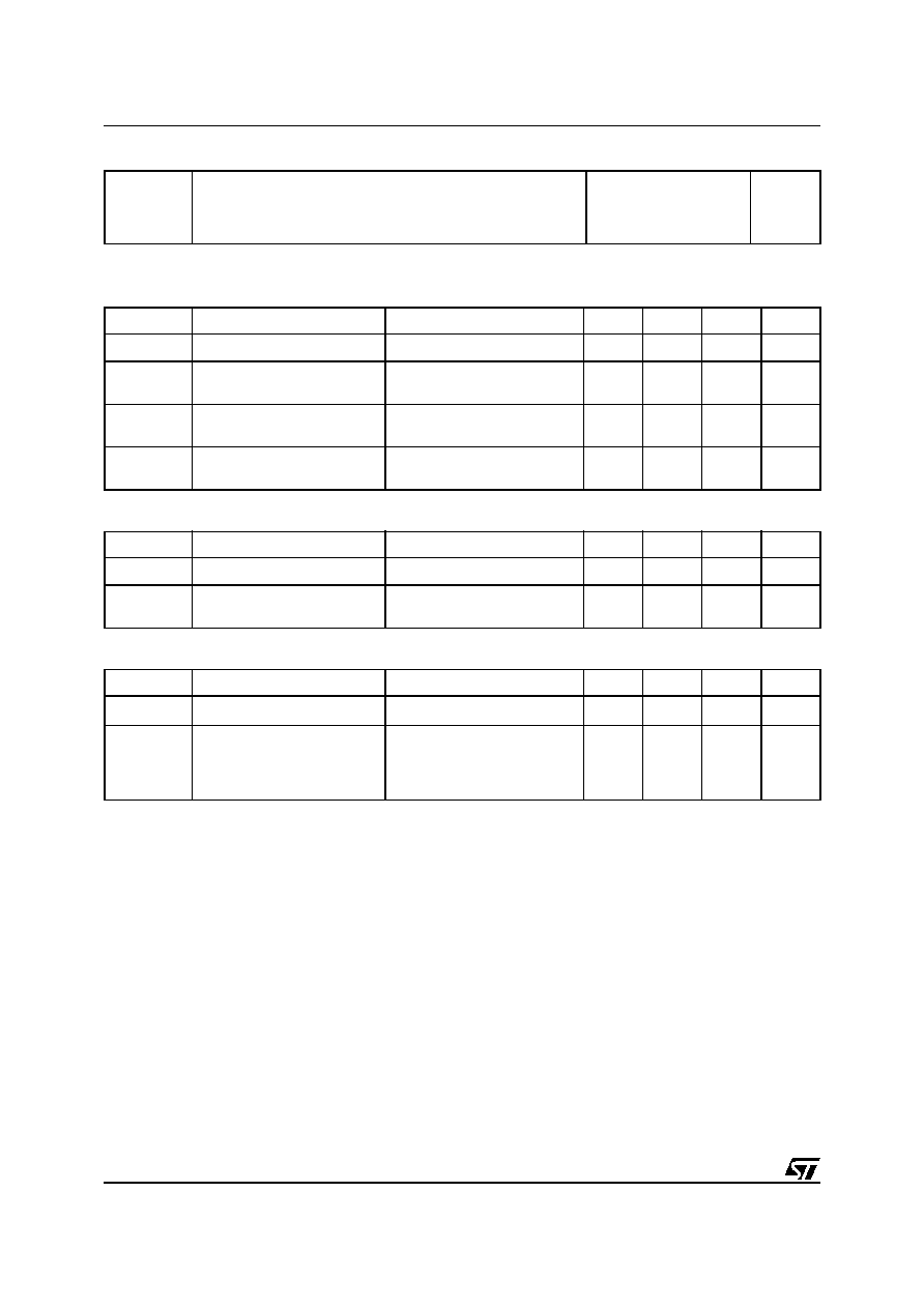
INTERNAL SCHEMATIC DIAGRAM
TYPICAL R
DS
(on) = 0.0125
100% AVALANCHE TESTED
LOW CAPACITANCE AND GATE CHARGE
175
o
C MAXIMUM JUNCTION
TEMPERATURE
DESCRIPTION
This fully clamped Mosfet is produced by using the latest
advanced Company's Mesh Overlay process which is
based on a novel strip layout.
The inherent benefits of the new technology coupled with
the extra clamping capabilities make this product
particularly suitable for the harshest operation conditions
such as those encountered in the automotive
environment. Any other application requiring extra
ruggedness is also recommended.
APPLICATIONS
ABS, SOLENOID DRIVERS
POWER TOOLS
Ordering Information
TYPE
V
DSS
R
DS(on)
I
D
STP62NS04Z
CLAMPED
<0.015
62 A
SALES TYPE
MARKING
PACKAGE
PACKAGING
STP62NS04Z
P62NS04Z
TO-220
TUBE
1
2
3
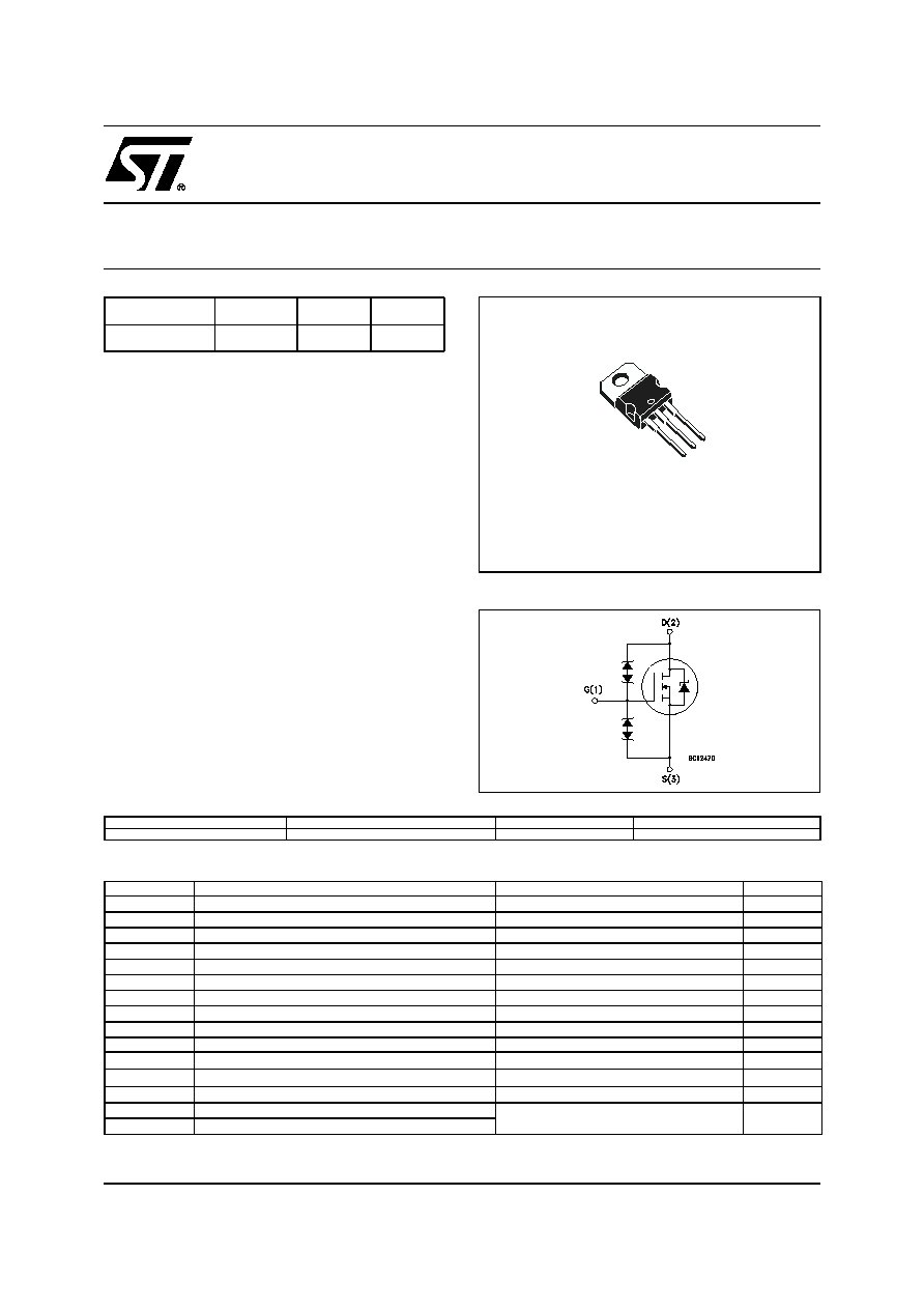
TO-220
ABSOLUTE MAXIMUM RATINGS
(
∑)
Pulse width limited by safe operating area.
(1) I
SD
40A, di/dt
100A/µs, V
DD
V
(BR)DSS
, T
j
T
JMAX
(2) Starting T
j
= 25
o
C, I
D
= 20A, V
DD
= 20V
Symbol
Parameter
Value
Unit
V
DS
Drain-source Voltage (V
GS
= 0)
CLAMPED
V
V
DG
Drain-gate Voltage
CLAMPED
V
V
GS
Gate- source Voltage
CLAMPED
V
I
D
Drain Current (continuous) at T
C
= 25∞C
62
A
I
D
Drain Current (continuous) at T
C
= 100∞C
37.5
A
I
DG
Drain Gate Current (continuous)
± 50
mA
I
GS
Gate SourceCurrent (continuous)
± 50
mA
I
DM
(
∑)
Drain Current (pulsed)
248
A
P
tot
Total Dissipation at T
C
= 25∞C
110
W
Derating Factor
0.74
W/∞C
dv/dt
(1)
Peak Diode Recovery voltage slope
8
V/ns
E
AS
(2)
Single Pulse Avalanche Energy
500
mJ
V
ESD
ESD (HBM - C = 100pF, R=1.5 k
)
8
kV
T
stg
Storage Temperature
-55 to 175
∞C
T
j
Operating Junction Temperature
STP62NS04Z
2/8
THERMAL DATA
ELECTRICAL CHARACTERISTICS (T
case
= 25 ∞C unless otherwise specified)
OFF
ON
(*)
DYNAMIC
Rthj-case
Rthj-amb
T
l
Thermal Resistance Junction-case
Thermal Resistance Junction-ambient
Maximum Lead Temperature For Soldering Purpose
(for 10 sec., 1.6mm from case)
Max
Max
1.36
62.5
300
∞C/W
∞C/W
∞C
Symbol
Parameter
Test Conditions
Min.
Typ.
Max.
Unit
V
(BR)DSS
Clamped Voltage
I
D
= 1 mA,
V
GS
= 0
33
V
I
DSS
Zero Gate Voltage
Drain Current (V
GS
= 0)
V
DS
= 16 V
10
µA
I
GSS
Gate-body Leakage
Current (V
DS
= 0)
V
GS
= ± 10 V
10
µA
V
GSS
Gate-Source
Breakdown Voltage
I
GS
= 100 µA
18
V
Symbol
Parameter
Test Conditions
Min.
Typ.
Max.
Unit
V
GS(th)
Gate Threshold Voltage
V
DS
= V
GS
I
D
= 250
µ
A
2
4
V
R
DS(on)
Static Drain-source On
Resistance
V
GS
= 10 V
I
D
= 30 A
12.5
15
m
Symbol
Parameter
Test Conditions
Min.
Typ.
Max.
Unit
g
fs
(*)
Forward Transconductance
V
DS
= 15 V
I
D
=30A
20
S
C
iss
C
oss
C
rss
Input Capacitance
Output Capacitance
Reverse Transfer
Capacitance
V
DS
= 25V, f = 1 MHz, V
GS
= 0
1330
420
135
pF
pF
pF
3/8
STP62NS04Z
SWITCHING ON
SWITCHING OFF
SOURCE DRAIN DIODE
(*)
Pulsed: Pulse duration = 300 µs, duty cycle 1.5 %.
(
∑
)
Pulse width limited by safe operating area.
Symbol
Parameter
Test Conditions
Min.
Typ.
Max.
Unit
t
d(on)
t
r
Turn-on Delay Time
Rise Time
V
DD
= 20 V
I
D
= 20 A
R
G
= 4.7
V
GS
= 10 V
(Resistive Load, Figure 3)
13
104
ns
ns
Q
g
Q
gs
Q
gd
Total Gate Charge
Gate-Source Charge
Gate-Drain Charge
V
DD
= 20 V I
D
= 40 A V
GS
= 10V
34
10
11.5
47
nC
nC
nC
Symbol
Parameter
Test Conditions
Min.
Typ.
Max.
Unit
t
d(off)
t
f
Turn-off Delay Time
Fall Time
V
DD
= 20 V
I
D
= 20 A
R
G
= 4.7
V
GS
= 10 V
(Resistive Load, Figure 3)
41
42
ns
ns
t
r(Voff)
t
f
t
c
Off-voltage Rise Time
Fall Time
Cross-over Time
V
clamp
= 30 V
I
D
= 40 A
R
G
= 4.7
,
V
GS
= 10 V
(Inductive Load, Figure 5)
30
54
90
ns
ns
ns
Symbol
Parameter
Test Conditions
Min.
Typ.
Max.
Unit
I
SD
I
SDM
(
∑)
Source-drain Current
Source-drain Current (pulsed)
62
248
A
A
V
SD
(*)
Forward On Voltage
I
SD
= 62 A
V
GS
= 0
1.5
V
t
rr
Q
rr
I
RRM
Reverse Recovery Time
Reverse Recovery Charge
Reverse Recovery Current
I
SD
= 40 A
di/dt = 100A/µs
V
DD
= 20 V
T
j
= 150∞C
(see test circuit, Figure 5)
45
65
2.9
ns
nC
A
ELECTRICAL CHARACTERISTICS (continued)
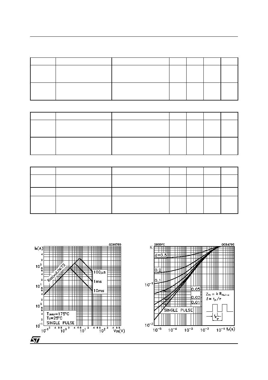
Safe Operating Area
Thermal Impedance
STP62NS04Z
4/8
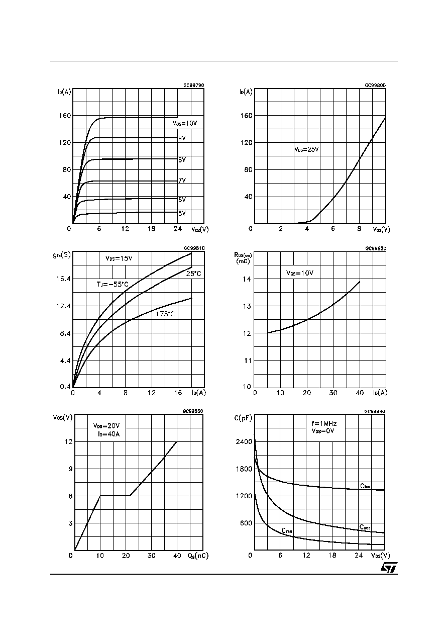
Output Characteristics
Transfer Characteristics
Transconductance
Static Drain-source On Resistance
Gate Charge vs Gate-source Voltage
Capacitance Variations
5/8
STP62NS04Z
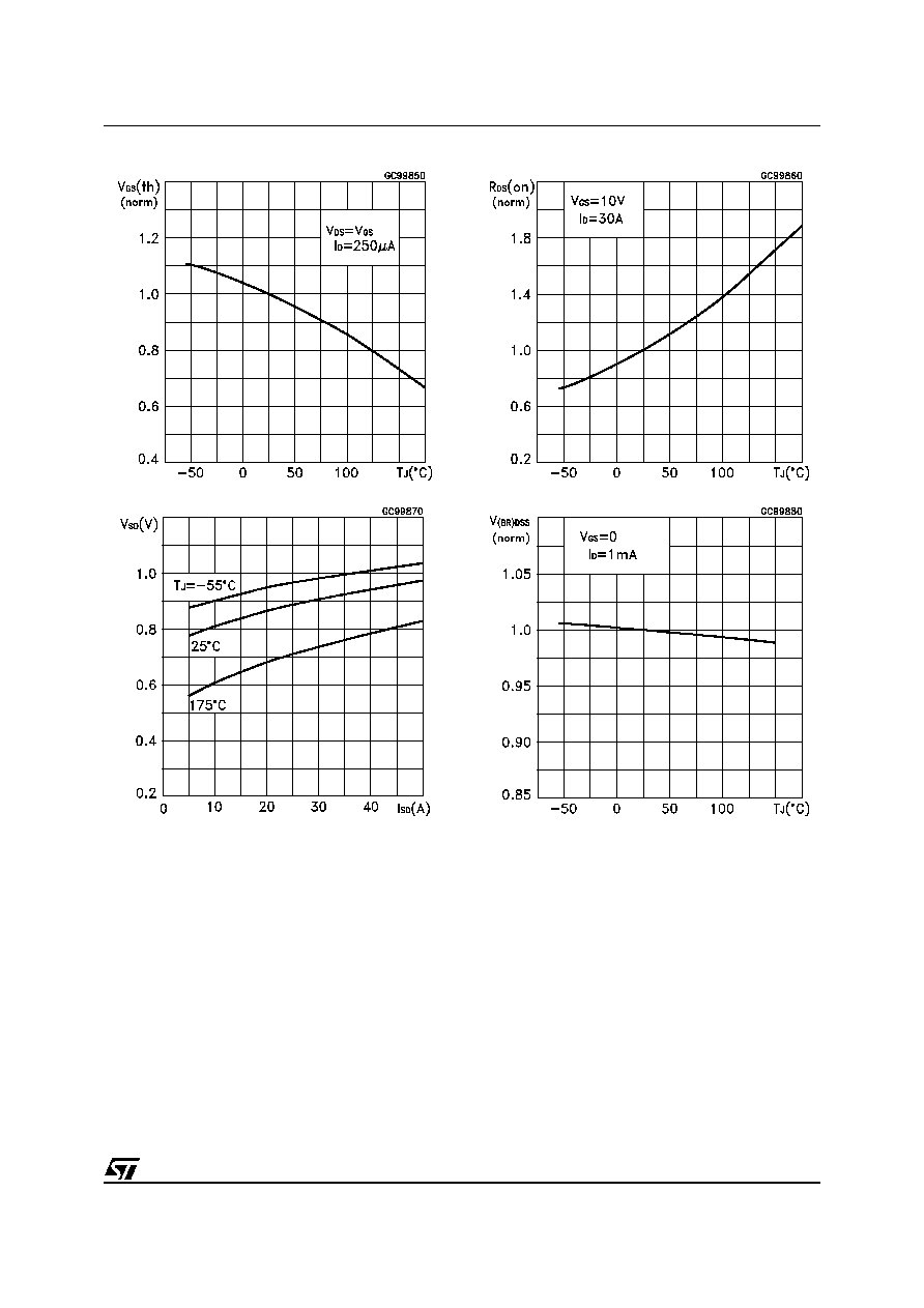
Normalized Gate Threshold Voltage vs Temperature
Normalized on Resistance vs Temperature
Source-drain Diode Forward Characteristics
Normalized Breakdown Voltage Temperature.
.
.
STP62NS04Z
6/8
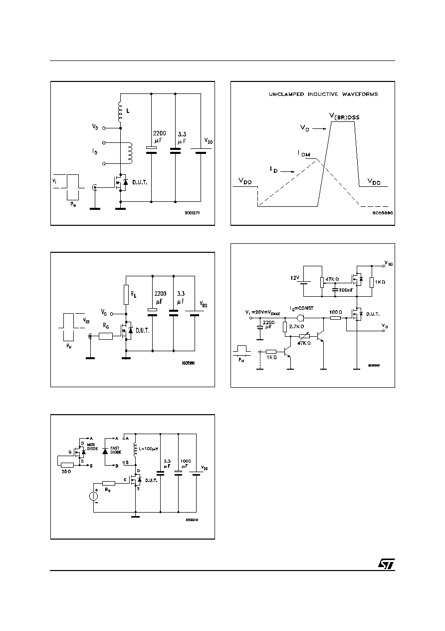
Fig. 1: Unclamped Inductive Load Test Circuit
Fig. 1: Unclamped Inductive Load Test Circuit
Fig. 2: Unclamped Inductive Waveform
Fig. 3: Switching Times Test Circuits For Resistive
Load
Fig. 4: Gate Charge test Circuit
Fig. 5: Test Circuit For Inductive Load Switching
And Diode Recovery Times
7/8
STP62NS04Z
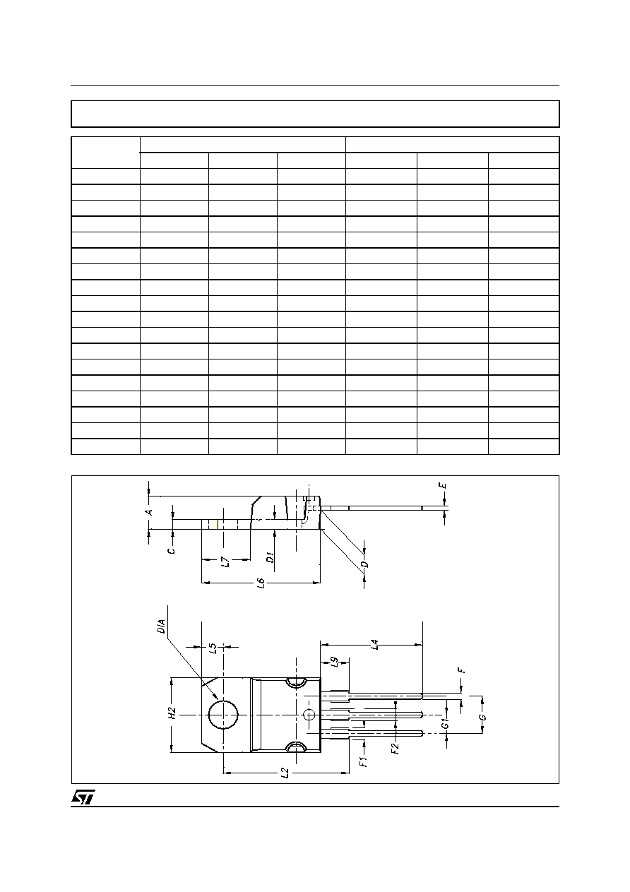
DIM.
mm.
inch.
MIN.
TYP. MAX.
MIN.
TYP. TYP.
A
4.4
4.6
0.173
0.181
C
1.23
1.32
0.048
0.051
D
2.40
2.72
0.094
0.107
D1
1.27
0.050
E
0.49
0.70
0.019
0.027
F
0.61
0.88
0.024
0.034
F1
1.14
1.70
0.044
0.067
F2
1.14
1.70
0.044
0.067
G
4.95
5.15
0.194
0.203
G1
2.40
2.70
0.094
0.106
H2
10
10.40
0.393
0.409
L2
16.10
16.40
16.73
0.633
0.645
0.658
L4
13
14
0.511
0.551
L5
2.65
2.95
0.104
0.116
L6
15.25
15.75
0.600
0.620
L7
6.20
6.60
0.244
0.260
L9
3.50
3.93
0.137
0.154
DIA
3.75
3.85
0.147
0.151
TO-220 MECHANICAL DATA

STP62NS04Z
8/8
Information furnished is believed to be accurate and reliable. However, STMicroelectronics assumes no responsibility for the consequences
of use of such information nor for any infringement of patents or other rights of third parties which may result from its use. No license is granted
by implication or otherwise under any patent or patent rights of STMicroelectronics. Specifications mentioned in this publication are subject
to change without notice. This publication supersedes and replaces all information previously supplied. STMicroelectronics products are not
authorized for use as critical components in life support devices or systems without express written approval of STMicroelectronics.
The ST logo is registered trademark of STMicroelectronics
All other names are the property of their respective owners.
©
2004 STMicroelectronics - All Rights Reserved
STMicroelectronics GROUP OF COMPANIES
Australia - Belgium - Brazil - Canada - China - Czech Republic - Finland - France - Germany - Hong Kong - India - Israel - Italy - Japan -
Malaysia - Malta - Morocco -Singapore - Spain - Sweden - Switzerland - United Kingdom - United States.
www.st.com