STP80N06-10
N - CHANNEL ENHANCEMENT MODE
"ULTRA HIGH DENSITY" POWER MOS TRANSISTOR
PRELIMINARY DATA
s
TYPICAL R
DS(on)
= 8.5 m
s
AVALANCHE RUGGED TECHNOLOGY
s
100% AVALANCE TESTED
s
HIGH CURRENT CAPABILITY
s
175
o
C OPERATING TEMPERATURE
s
HIGH dV/dt RUGGEDNESS
s
APPLICATION ORIENTED
CHARACTERIZATION
APPLICATIONS
s
HIGH CURRENT, HIGH SPEED SWITCHING
s
PWM MOTOR CONTROL
s
DC-DC & DC-AC CONVERTER
s
SYNCROUNOUS RECTIFICATION
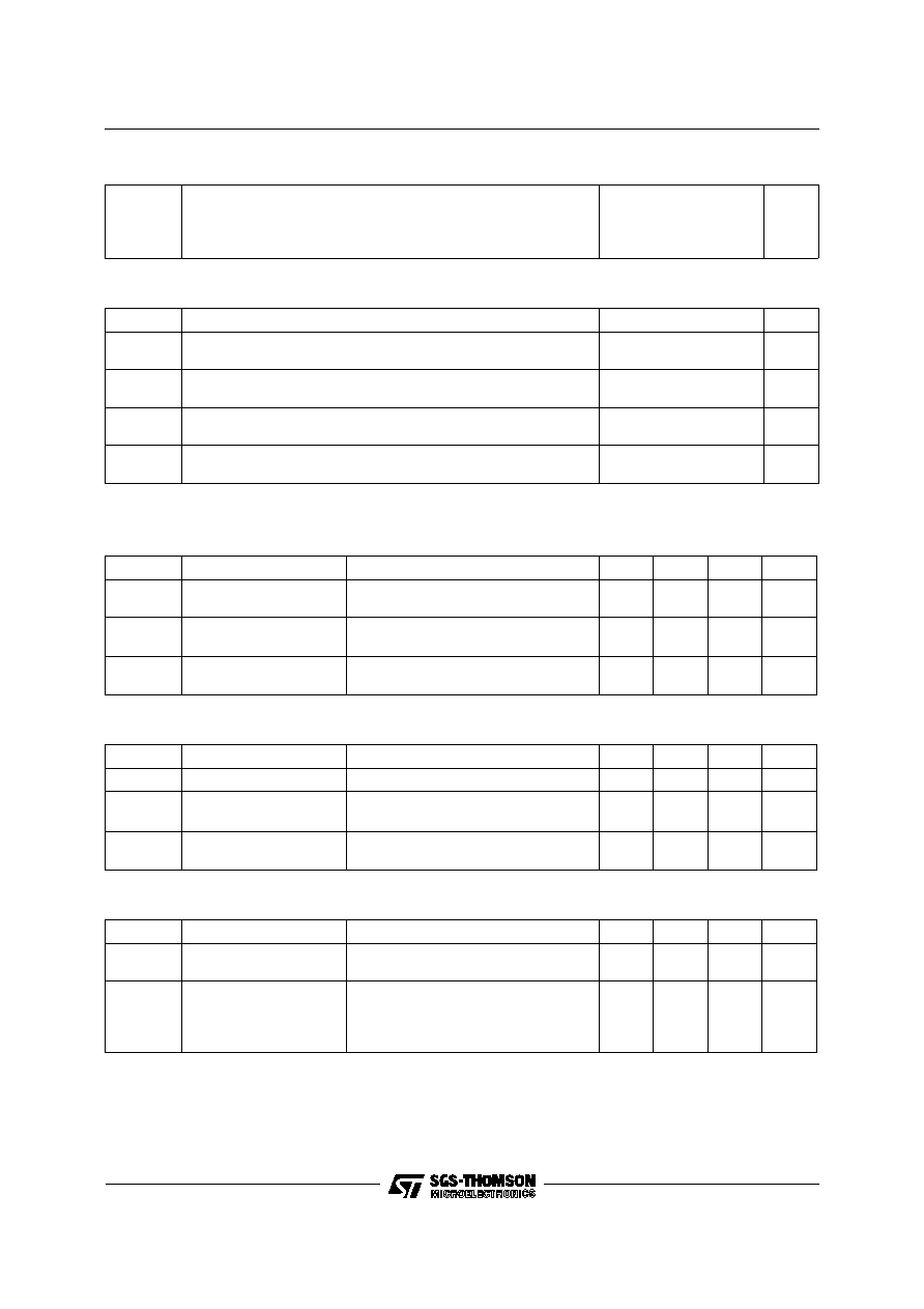
INTERNAL SCHEMATIC DIAGRAM
ABSOLUTE MAXIMUM RATINGS
Symbol
Parameter
Value
Unit
V
DS
Drain-source Voltage (V
GS
= 0)
60
V
V
DGR
Drain- gate Voltage (R
GS
= 20 k
)
60
V
V
GS
Gate-source Voltage
±
20
V
I
D
Drain Current (continuous) at T
c
= 25
o
C
80
A
I
D
Drain Current (continuous) at T
c
= 100
o
C
60
A
I
DM
(
∑
)
Drain Current (pulsed)
320
A
P
tot
Total Dissipation at T
c
= 25
o
C
150
W
Derating Factor
1
W/
o
C
dV/dt(
1
)
Peak Diode Recovery voltage slope
5
V/ns
T
stg
Storage Temperature
-65 to 175
o
C
T
j
Max. Operating Junction Temperature
175
o
C
(
∑
) Pulse width limited by safe operating area
TYPE
V
DSS
R
DS(on)
I
D
STP80N06-10
60 V
< 0.010
80 A
March 1996
1
2
3
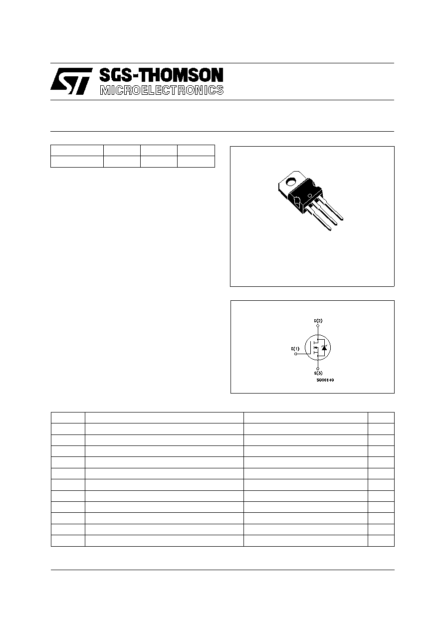
TO-220
1/5
THERMAL DATA
R
thj-case
R
thj-amb
R
thc-sink
T
l
Thermal Resistance Junction-case Max
Thermal Resistance Junction-ambient Max
Thermal Resistance Case-sink Typ
Maximum Lead Temperature For Soldering Purpose
1
62.5
0.5
300
o
C/W
o
C/W
o
C/W
o
C
AVALANCHE CHARACTERISTICS
Symbol
Parameter
Max Value
Unit
I
AR
Avalanche Current, Repetitive or Not-Repetitive
(pulse width limited by T
j
max,
< 1%)
60
A
E
AS
Single Pulse Avalanche Energy
(starting T
j
= 25
o
C, I
D
= I
AR
, V
DD
= 25 V)
600
mJ
E
AR
Repetitive Avalanche Energy
(pulse width limited by T
j
max,
< 1%)
150
mJ
I
AR
Avalanche Current, Repetitive or Not-Repetitive
(T
c
= 100
o
C, pulse width limited by T
j
max,
< 1%)
60
A
ELECTRICAL CHARACTERISTICS (T
case
= 25
o
C unless otherwise specified)
OFF
Symbol
Parameter
Test Conditions
Min.
Typ.
Max.
Unit
V
(BR)DSS
Drain-source
Breakdown Voltage
I
D
= 250
µ
A V
GS
= 0
60
V
I
DSS
Zero Gate Voltage
Drain Current (V
GS
= 0)
V
DS
= Max Rating
V
DS
= Max Rating x 0.8 T
c
= 125
o
C
250
1000
µ
A
µ
A
I
GSS
Gate-body Leakage
Current (V
DS
= 0)
V
GS
=
±
20 V
±
100
nA
ON (
)
Symbol
Parameter
Test Conditions
Min.
Typ.
Max.
Unit
V
GS(th)
Gate Threshold Voltage V
DS
= V
GS
I
D
= 250
µ
A
2
3
4
V
R
DS(on)
Static Drain-source On
Resistance
V
GS
= 10V I
D
= 40 A
V
GS
= 10V I
D
= 40 A T
c
= 100
o
C
0.0085
0.01
0.02
I
D(on )
On State Drain Current
V
DS
> I
D(on)
x R
DS(on)max
V
GS
= 10 V
80
A
DYNAMIC
Symbol
Parameter
Test Conditions
Min.
Typ.
Max.
Unit
g
fs
(
)
Forward
Transconductance
V
DS
> I
D(on)
x R
DS(on)max
I
D
= 40 A
25
S
C
iss
C
oss
C
rss
Input Capacitance
Output Capacitance
Reverse Transfer
Capacitance
V
DS
= 25 V f = 1 MHz V
GS
= 0
5900
900
230
pF
pF
pF
STP80N06-10
2/5
ELECTRICAL CHARACTERISTICS (continued)
SWITCHING ON
Symbol
Parameter
Test Conditions
Min.
Typ.
Max.
Unit
t
d(on)
t
r
Turn-on Time
Rise Time
V
DD
= 30 V I
D
= 40 A
R
G
= 4.7
V
GS
= 10 V
(see test circuit, figure 3)
32
160
42
200
ns
ns
(di/dt)
on
Turn-on Current Slope
V
DD
= 48 V I
D
= 80 A
R
G
=50
V
GS
= 10 V
(see test circuit, figure 5)
240
A/
µ
s
Q
g
Q
gs
Q
gd
Total Gate Charge
Gate-Source Charge
Gate-Drain Charge
V
DD
= 40 V I
D
= 80 A V
GS
= 10 V
230
30
60
280
nC
nC
nC
SWITCHING OFF
Symbol
Parameter
Test Conditions
Min.
Typ.
Max.
Unit
t
r(Voff)
t
f
t
c
Off-voltage Rise Time
Fall Time
Cross-over Time
V
DD
= 48 V I
D
= 40 A
R
G
= 4.7
V
GS
= 10 V
(see test circuit, figure 5)
35
175
240
46
230
300
ns
ns
ns
SOURCE DRAIN DIODE
Symbol
Parameter
Test Conditions
Min.
Typ.
Max.
Unit
I
SD
I
SDM
(
∑
)
Source-drain Current
Source-drain Current
(pulsed)
80
320
A
A
V
SD
(
)
Forward On Voltage
I
SD
= 80 A V
GS
= 0
1.5
V
t
rr
Q
rr
I
RRM
Reverse Recovery
Time
Reverse Recovery
Charge
Reverse Recovery
Current
I
SD
= 80 A di/dt = 100 A/
µ
s
V
R
= 30 V T
j
= 150
o
C
(see test circuit, figure 5)
125
0.6
10
ns
µ
C
A
(
) Pulsed: Pulse duration = 300
µ
s, duty cycle 1.5 %
(
∑
) Pulse width limited by safe operating area
(
1
) I
SD
60 A, di/dt
200 A/
µ
s, V
DD
V
(BR)DSS
, T
J
T
JMAX
STP80N06-10
3/5
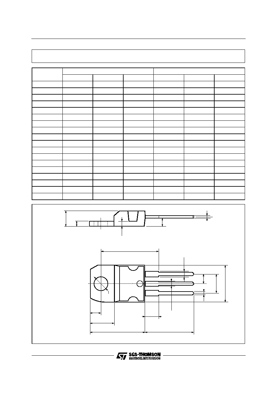
DIM.
mm
inch
MIN.
TYP.
MAX.
MIN.
TYP.
MAX.
A
4.40
4.60
0.173
0.181
C
1.23
1.32
0.048
0.051
D
2.40
2.72
0.094
0.107
D1
1.27
0.050
E
0.49
0.70
0.019
0.027
F
0.61
0.88
0.024
0.034
F1
1.14
1.70
0.044
0.067
F2
1.14
1.70
0.044
0.067
G
4.95
5.15
0.194
0.203
G1
2.4
2.7
0.094
0.106
H2
10.0
10.40
0.393
0.409
L2
16.4
0.645
L4
13.0
14.0
0.511
0.551
L5
2.65
2.95
0.104
0.116
L6
15.25
15.75
0.600
0.620
L7
6.2
6.6
0.244
0.260
L9
3.5
3.93
0.137
0.154
DIA.
3.75
3.85
0.147
0.151
L6
A
C
D
E
D1
F
G
L7
L2
Dia.
F1
L5
L4
H2
L9
F2
G1
TO-220 MECHANICAL DATA
P011C
STP80N06-10
4/5

Information furnished is believed to be accurate and reliable. However, SGS-THOMSON Microelectronics assumes no responsability for the
consequences of use of such information nor for any infringement of patents or other rights of third parties which may results from its use. No
license is granted by implication or otherwise under any patent or patent rights of SGS-THOMSON Microelectronics. Specifications mentioned
in this publication are subject to change without notice. This publication supersedes and replaces all information previously supplied.
SGS-THOMSON Microelectronics products are not authorized for use as critical components in life support devices or systems without express
written approval of SGS-THOMSON Microelectonics.
© 1995 SGS-THOMSON Microelectronics - All Rights Reserved
SGS-THOMSON Microelectronics GROUP OF COMPANIES
Australia - Brazil - France - Germany - Hong Kong - Italy - Japan - Korea - Malaysia - Malta - Morocco - The Netherlands -
Singapore - Spain - Sweden - Switzerland - Taiwan - Thailand - United Kingdom - U.S.A
. . .
STP80N06-10
5/5