STP80NF03L-04
N-CHANNEL 30V - 0.0034
- 80A TO-220
STripFET
TM
POWER MOSFET
PRELIMINARY DATA
s
TYPICAL R
DS(on)
= 0.0034
s
EXCEPTIONAL dv/dt CAPABILITY
s
100% AVALANCHE TESTED
s
LOW GATE CHARGE 100
o
C
s
APPLICATION ORIENTED
CHARACTERIZATION
DESCRIPTION
This Power Mosfet is the latest development of
STMicroelectronics
unique
"Single
Feature
Size
TM
"
strip-based
process.
The
resulting
transistor shows extremely high packing density
for
low
on-resistance,
rugged
avalance
characteristics and less critical alignment steps
therefore
a
remarkable
manufacturing
reproducibility.
APPLICATIONS
s
HIGH CURRENT, HIGH SPEED SWITCHING
s
SOLENOID AND RELAY DRIVERS
s
MOTOR CONTROL, AUDIO AMPLIFIERS
s
DC-DC & DC-AC CONVERTERS
s
AUTOMOTIVE ENVIRONMENT (INJECTION,
ABS, AIR-BAG, LAMPDRIVERS, Etc. )
�
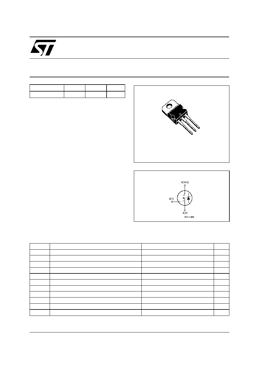
INTERNAL SCHEMATIC DIAGRAM
November 1999
T YPE
V
DSS
R
DS(on)
I
D
STP80NF03L-04
30 V
< 0. 004
80 A
1
2
3
TO-220
ABSOLUTE MAXIMUM RATINGS
Symb ol
Parameter
Value
Unit
V
DS
Drain-source Voltage (V
GS
= 0)
30
V
V
DGR
Drain- gate Voltage (R
GS
= 20 k
)
30
V
V
G S
G ate-source Volt age
�
20
V
I
D
(
��)
Drain Current (continuous) at T
c
= 25
o
C
80
A
I
D
Drain Current (continuous) at T
c
= 100
o
C
56
A
I
DM
(
�)
Drain Current (pulsed)
320
A
P
tot
T otal Dissipation at T
c
= 25
o
C
210
W
Derating Factor
1.43
W /
o
C
E
AS
(
1
)
Single Pulse Avalanche Energy
2
J
T
st g
Storage Temperature
-65 to 175
o
C
T
j
Max. Operating Junction Temperature
175
o
C
(
�)
Pulse width limited by safe operating area
(
��)
Current limited by package
(
1
)
starting T
j
= 25
o
C, I
D
=40A , V
DD
=15V
1/6

THERMAL DATA
R
thj -case
Rthj -amb
R
thc-sink
T
l
Thermal Resistance Junction-case
Max
Thermal Resistance Junction-ambient
Max
Thermal Resistance Case-sink
Typ
Maximum Lead Temperature F or Soldering Purpose
0.7
62.5
0.5
300
o
C/W
oC/ W
o
C/W
o
C
ELECTRICAL CHARACTERISTICS (T
case
= 25
o
C unless otherwise specified)
OFF
Symbo l
Parameter
Test Con ditions
Min.
Typ.
Max.
Unit
V
(BR)DSS
Drain-source
Breakdown Voltage
I
D
= 250
�
A
V
GS
= 0
30
V
I
DSS
Zero Gat e Voltage
Drain Current (V
GS
= 0)
V
DS
= Max Rat ing
V
DS
= Max Rat ing
T
c
=125
o
C
1
10
�
A
�
A
I
G SS
Gat e-body Leakage
Current (V
DS
= 0)
V
GS
=
�
20 V
�
100
nA
ON (
)
Symbo l
Parameter
Test Con ditions
Min.
Typ.
Max.
Unit
V
G S(th)
Gat e Threshold Voltage V
DS
= V
GS
I
D
= 250
�
A
1
1.7
2. 5
V
R
DS(on)
Static Drain-source On
Resistance
V
GS
= 10V
I
D
= 40 A
V
GS
= 4. 5V
I
D
= 40 A
0.0034
0.0042
0.004
0.0055
I
D(o n)
On State Drain Current
V
DS
> I
D(o n)
x R
DS(on )ma x
V
GS
= 10 V
80
A
DYNAMIC
Symbo l
Parameter
Test Con ditions
Min.
Typ.
Max.
Unit
g
f s
(
)
Forward
Transconductance
V
DS
> I
D(o n)
x R
DS(on )ma x
I
D
=15 A
50
S
C
iss
C
os s
C
rss
Input Capacitance
Out put Capacitance
Reverse Transfer
Capacitance
V
DS
= 25 V
f = 1 MHz
V
GS
= 0
7000
1700
600
pF
pF
pF
STP80NF03L-04
2/6

ELECTRICAL CHARACTERISTICS (continued)
SWITCHING ON
Symbo l
Parameter
Test Con ditions
Min.
Typ.
Max.
Unit
t
d(on)
t
r
Turn-on Delay T ime
Rise Time
V
DD
= 15 V
I
D
= 40 A
R
G
= 4.7
V
G S
= 4.5 V
(Resistive Load, see fig. 3)
50
275
ns
ns
Q
g
Q
gs
Q
gd
Tot al G ate Charge
Gat e-Source Charge
Gat e-Drain Charge
V
DD
= 24 V I
D
= 80 A V
GS
= 4.5 V
120
37
58
160
nC
nC
nC
SWITCHING OFF
Symbo l
Parameter
Test Con ditions
Min.
Typ.
Max.
Unit
t
d(of f)
t
f
Turn-off Delay T ime
Fall T ime
V
DD
= 15 V
I
D
= 40 A
R
G
= 4.7
V
G S
= 4.5 V
(Resistive Load, see fig. 3)
230
190
ns
ns
t
r (Voff)
t
f
t
c
Off -volt age Rise T ime
Fall T ime
Cross-over Time
V
clamp
= 24 V
I
D
= 80 A
R
G
= 4.7
V
G S
= 4.5 V
(Induct ive Load, see fig. 5)
175
280
470
ns
ns
ns
SOURCE DRAIN DIODE
Symbo l
Parameter
Test Con ditions
Min.
Typ.
Max.
Unit
I
SD
I
SDM
(
�
)
Source-drain Current
Source-drain Current
(pulsed)
80
320
A
A
V
SD
(
)
Forward On Voltage
I
SD
= 80 A
V
GS
= 0
1. 5
V
t
rr
Q
rr
I
RRM
Reverse Recovery
Time
Reverse Recovery
Charge
Reverse Recovery
Current
I
SD
= 80 A
di/dt = 100 A/
�
s
V
DD
= 20 V
T
j
= 150
o
C
(see t est circuit, f ig. 5)
88
0.176
4.4
ns
�
C
A
(
) Pulsed: Pulse duration = 300
�
s, duty cycle 1.5 %
(
�
) Pulse width limited by safe operating area
STP80NF03L-04
3/6
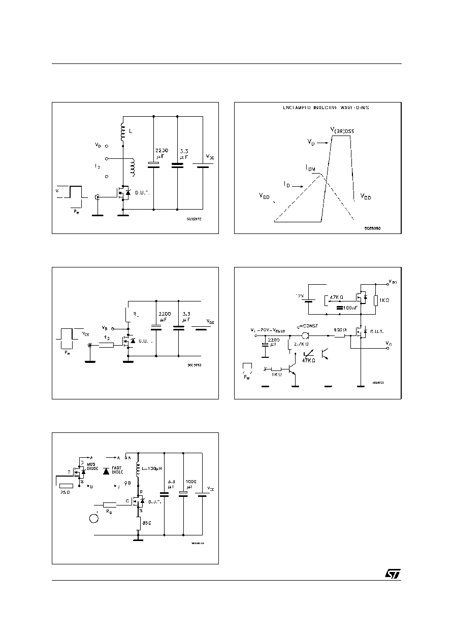
Fig. 1: Unclamped Inductive Load Test Circuit
Fig. 3: Switching Times Test Circuits For
Resistive Load
Fig. 2: Unclamped Inductive Waveform
Fig. 4: Gate Charge test Circuit
Fig. 5: Test Circuit For Inductive Load Switching
And Diode Recovery Times
STP80NF03L-04
4/6
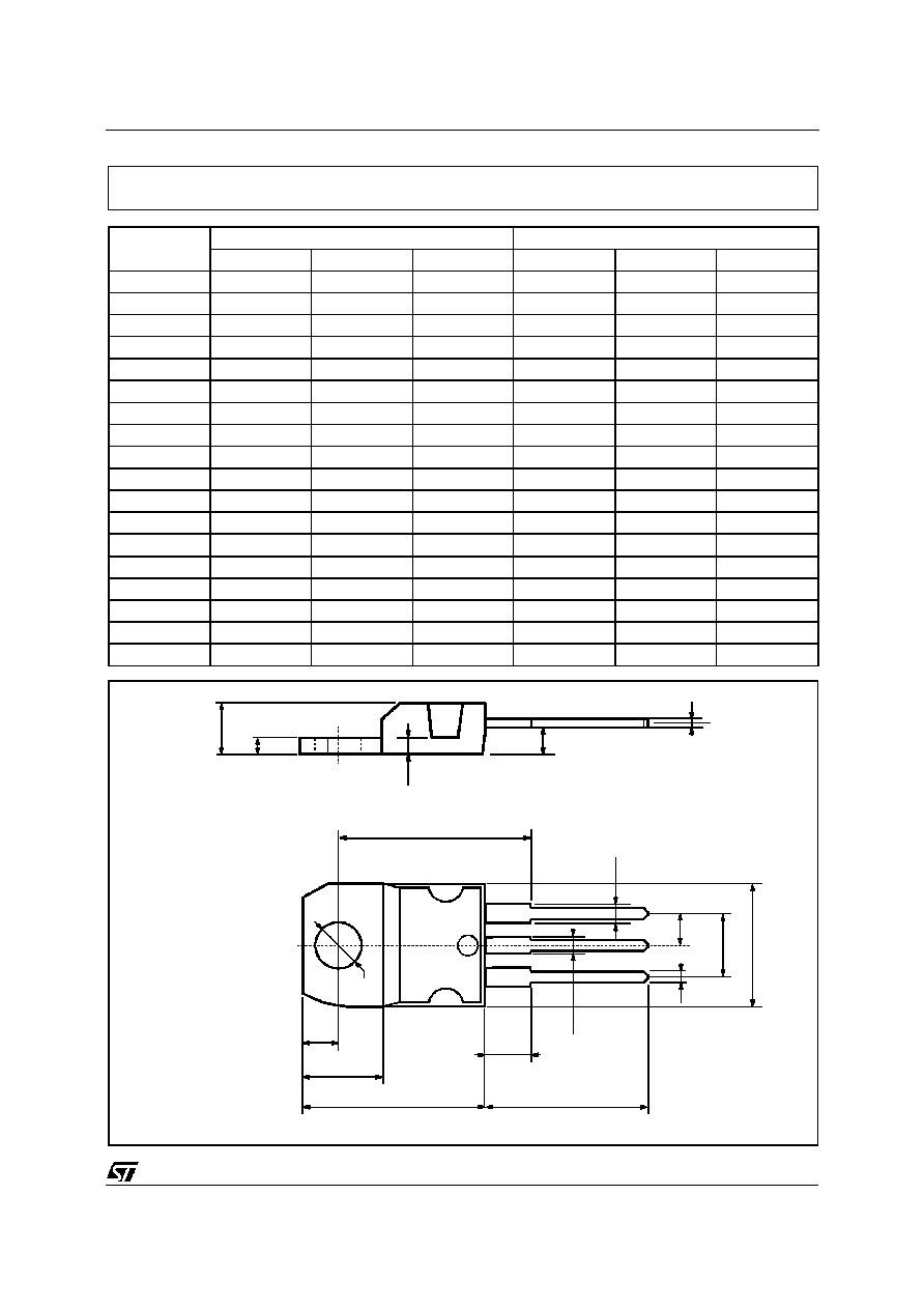
DIM.
mm
inch
MIN.
TYP.
MAX.
MIN.
TYP.
MAX.
A
4.40
4.60
0.173
0.181
C
1.23
1.32
0.048
0.051
D
2.40
2.72
0.094
0.107
D1
1.27
0.050
E
0.49
0.70
0.019
0.027
F
0.61
0.88
0.024
0.034
F1
1.14
1.70
0.044
0.067
F2
1.14
1.70
0.044
0.067
G
4.95
5.15
0.194
0.203
G1
2.4
2.7
0.094
0.106
H2
10.0
10.40
0.393
0.409
L2
16.4
0.645
L4
13.0
14.0
0.511
0.551
L5
2.65
2.95
0.104
0.116
L6
15.25
15.75
0.600
0.620
L7
6.2
6.6
0.244
0.260
L9
3.5
3.93
0.137
0.154
DIA.
3.75
3.85
0.147
0.151
L6
A
C
D
E
D1
F
G
L7
L2
Dia.
F1
L5
L4
H2
L9
F2
G1
TO-220 MECHANICAL DATA
P011C
STP80NF03L-04
5/6