1/9
September 2002
STP80NF10
STP80NF10FP
N-CHANNEL 100V - 0.012
- 80A TO-220/TO-220FP
LOW GATE CHARGE STripFETTMII POWER MOSFET
(1) I
SD
80A, di/dt
300A/µs, V
DD
V
(BR)DSS
, T
j
T
JMAX.
(2) Starting T
j
= 25∞C, I
D
= 80A, V
DD
= 50V
s
TYPICAL R
DS
(on) = 0.012
s
EXCEPTIONAL dv/dt CAPABILITY
s
100% AVALANCHE TESTED
s
APPLICATION ORIENTED
CHARACTERIZATION
DESCRIPTION
This Power MOSFET series realized with STMicro-
electronics unique STripFET process has specifical-
ly been designed to minimize input capacitance and
gate charge. It is therefore suitable as primary
switch in advanced high-efficiency isolated DC-DC
converters for Telecom and Computer application. It
is also intended for any application with low gate
charge drive requirements.
APPLICATIONS
s
HIGH-EFFICIENCY DC-DC CONVERTERS
s
UPS AND MOTOR CONTROL
ABSOLUTE MAXIMUM RATINGS
(
q
) Pulse width limited by safe operating area
(*) Limited by Package
TYPE
V
DSS
R
DS(on)
I
D
STP80NF10
STP80NF10FP
100 V
100 V
< 0.015
< 0.015
80 A
38 A
Symbol
Parameter
Value
Unit
STP80NF10
STP80NF10FP
V
DS
Drain-source Voltage (V
GS
= 0)
100
V
V
DGR
Drain-gate Voltage (R
GS
= 20 k
)
100
V
V
GS
Gate- source Voltage
±20
V
I
D
(*)
Drain Current (continuous) at T
C
= 25∞C
80
38
A
I
D
Drain Current (continuous) at T
C
= 100∞C
66
27
A
I
DM
(
l
)
Drain Current (pulsed)
320
152
A
P
TOT
Total Dissipation at T
C
= 25∞C
300
45
W
Derating Factor
2
0.3
W/∞C
dv/dt (1)
Peak Diode Recovery voltage slope
9
V/ns
E
AS
(2)
Single Pulse Avalanche Energy
360
mJ
V
ISO
Insulation Withstand Voltage (DC)
-
2500
V
T
stg
Storage Temperature
≠ 55 to 175
∞C
T
j
Max. Operating Junction Temperature
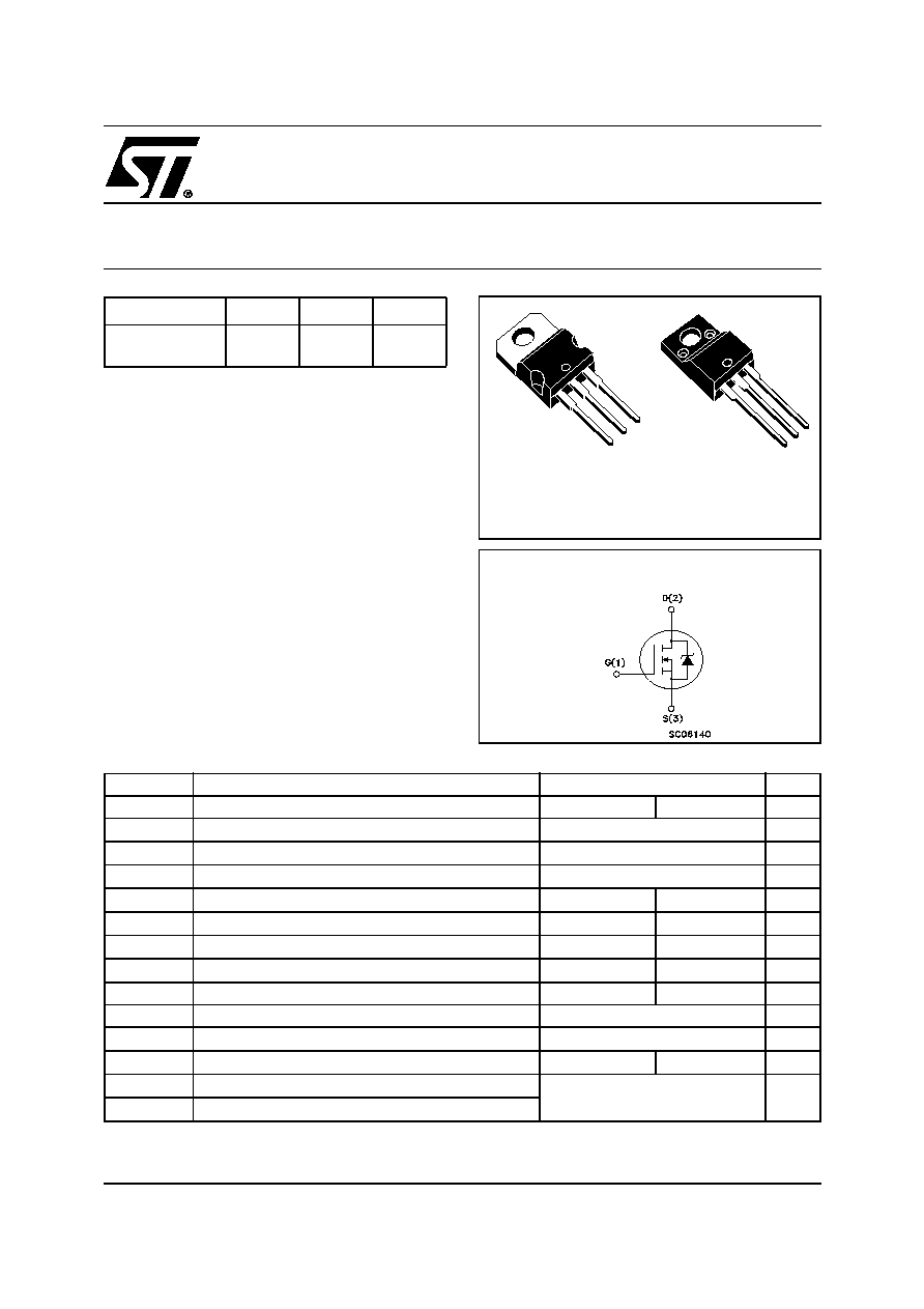
TO-220
1
2
3
1
2
3
TO-220FP
INTERNAL SCHEMATIC DIAGRAM
STP80NF10/STP80NF10FP
2/9
THERMAL DATA
ELECTRICAL CHARACTERISTICS (T
CASE
= 25 ∞C UNLESS OTHERWISE SPECIFIED)
OFF
ON
(1)
DYNAMIC
TO-220
TO-220FP
Rthj-case
Thermal Resistance Junction-case Max
0.5
3.33
∞C/W
Rthj-amb
Thermal Resistance Junction-ambient Max
62.5
∞C/W
T
l
Maximum Lead Temperature For Soldering Purpose
300
∞C
Symbol
Parameter
Test Conditions
Min.
Typ.
Max.
Unit
V
(BR)DSS
Drain-source
Breakdown Voltage
I
D
= 250 µA, V
GS
= 0
100
V
I
DSS
Zero Gate Voltage
Drain Current (V
GS
= 0)
V
DS
= Max Rating
1
µA
V
DS
= Max Rating, T
C
= 125 ∞C
10
µA
I
GSS
Gate-body Leakage
Current (V
DS
= 0)
V
GS
= ±20V
±100
nA
Symbol
Parameter
Test Conditions
Min.
Typ.
Max.
Unit
V
GS(th)
Gate Threshold Voltage
V
DS
= V
GS
, I
D
= 250µA
2
3
4
V
R
DS(on)
Static Drain-source On
Resistance
V
GS
= 10V, I
D
= 40 A
0.012
0.015
Symbol
Parameter
Test Conditions
Min.
Typ.
Max.
Unit
g
fs
(1)
Forward Transconductance
V
DS
=25V
,
I
D
=40 A
80
S
C
iss
Input Capacitance
V
DS
= 25V, f = 1 MHz, V
GS
= 0
4300
pF
C
oss
Output Capacitance
600
pF
C
rss
Reverse Transfer
Capacitance
230
pF
3/9
STP80NF10/STP80NF10FP
ELECTRICAL CHARACTERISTICS (CONTINUED)
SWITCHING ON
SWITCHING OFF
SOURCE DRAIN DIODE
Note: 1. Pulsed: Pulse duration = 300 µs, duty cycle 1.5 %.
2. Pulse width limited by safe operating area.
Symbol
Parameter
Test Conditions
Min.
Typ.
Max.
Unit
t
d(on)
Turn-on Delay Time
V
DD
= 50V, I
D
= 40A
R
G
= 4.7
V
GS
= 10V
(see test circuit, Figure 3)
40
ns
t
r
Rise Time
145
ns
Q
g
Q
gs
Q
gd
Total Gate Charge
Gate-Source Charge
Gate-Drain Charge
V
DD
= 80V, I
D
= 80A,
V
GS
= 10V
140
23
51
189
nC
nC
nC
Symbol
Parameter
Test Conditions
Min.
Typ.
Max.
Unit
t
d(off)
t
f
Turn-off-Delay Time
Fall Time
V
DD
= 50V, I
D
= 40A,
R
G
= 4.7
,
V
GS
= 10V
(see test circuit, Figure 3)
134
115
ns
ns
Symbol
Parameter
Test Conditions
Min.
Typ.
Max.
Unit
I
SD
Source-drain Current
80
A
I
SDM
(2)
Source-drain Current (pulsed)
320
A
V
SD
(1)
Forward On Voltage
I
SD
= 80A, V
GS
= 0
1.3
V
t
rr
Q
rr
I
RRM
Reverse Recovery Time
Reverse Recovery Charge
Reverse Recovery Current
I
SD
= 80A, di/dt = 100A/µs,
V
DD
= 50V, T
j
= 150∞C
(see test circuit, Figure 5)
155
0.85
11
ns
µC
A
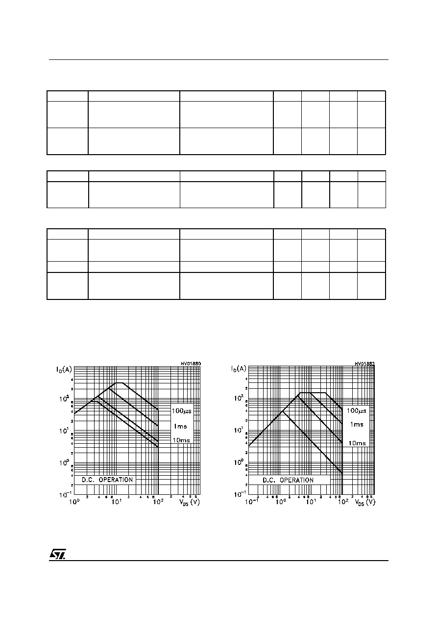
Safe Operating Area for TO-220FP
Safe Operating Area for TO-220
STP80NF10/STP80NF10FP
4/9
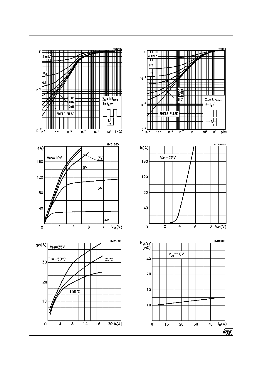
Thermal Impedence for TO-220FP
Thermal Impedence for TO-220
Static Drain-source On Resistance
Output Characteristics
Transconductance
Transfer Characteristics
5/9
STP80NF10/STP80NF10FP
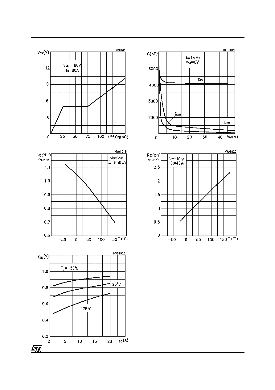
Normalized On Resistance vs Temperature
Capacitance Variations
Normalized Gate Thereshold Voltage vs Temp.
Source-drain Diode Forward Characteristics
Gate Charge vs Gate-source Voltage
STP80NF10/STP80NF10FP
6/9
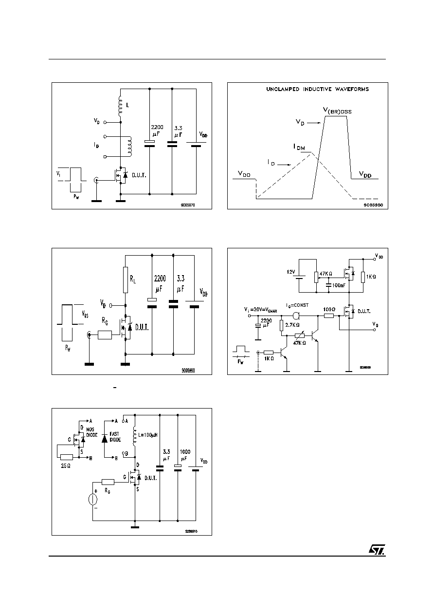
Fig. 5: Test Circuit For Inductive Load Switching
And Diode Recovery Times
Fig. 4: Gate Charge test Circuit
Fig. 2: Unclamped Inductive Waveform
Fig. 1: Unclamped Inductive Load Test Circuit
Fig. 3: Switching Times Test Circuit For
Resistive Load
7/9
STP80NF10/STP80NF10FP
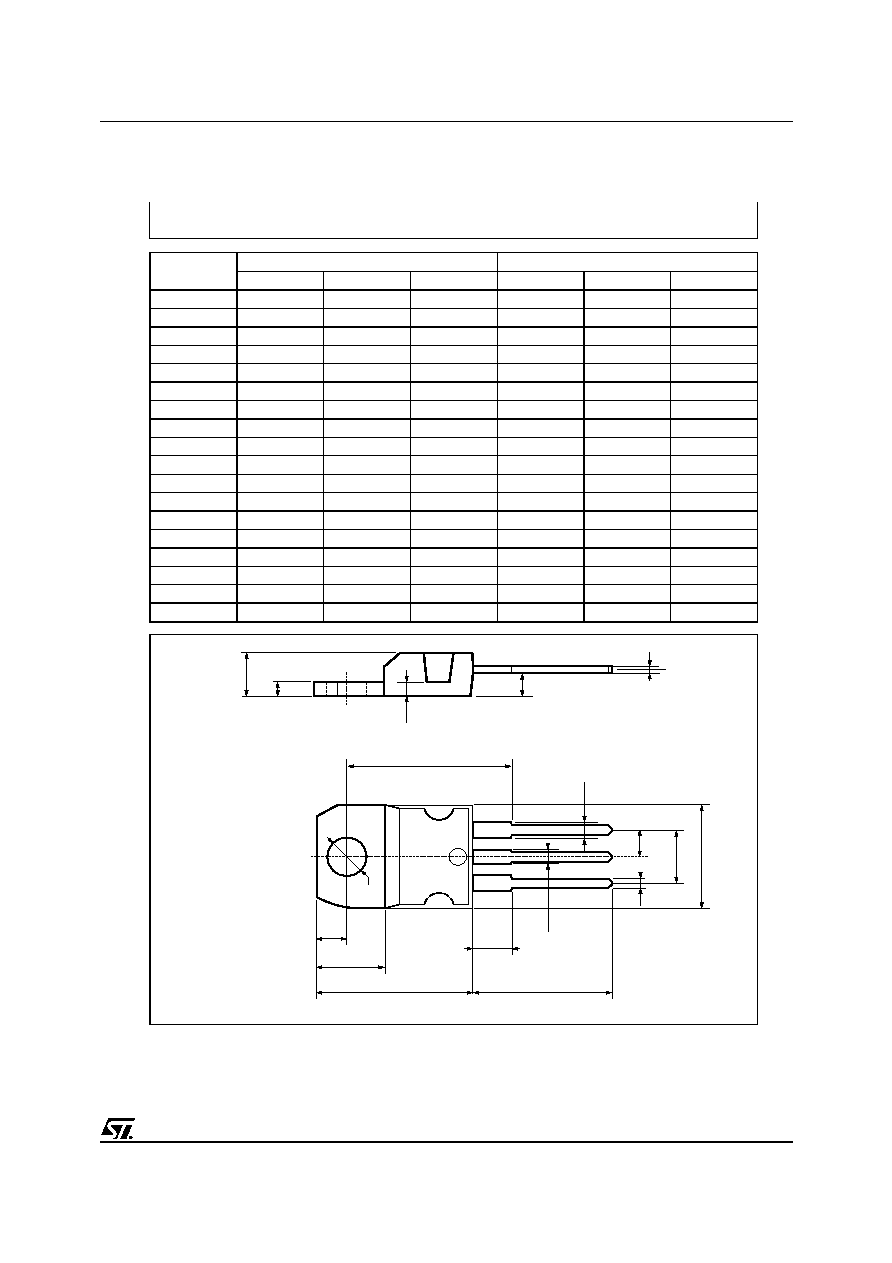
DIM.
mm
inch
MIN.
TYP.
MAX.
MIN.
TYP.
MAX.
A
4.40
4.60
0.173
0.181
C
1.23
1.32
0.048
0.051
D
2.40
2.72
0.094
0.107
D1
1.27
0.050
E
0.49
0.70
0.019
0.027
F
0.61
0.88
0.024
0.034
F1
1.14
1.70
0.044
0.067
F2
1.14
1.70
0.044
0.067
G
4.95
5.15
0.194
0.203
G1
2.4
2.7
0.094
0.106
H2
10.0
10.40
0.393
0.409
L2
16.4
0.645
L4
13.0
14.0
0.511
0.551
L5
2.65
2.95
0.104
0.116
L6
15.25
15.75
0.600
0.620
L7
6.2
6.6
0.244
0.260
L9
3.5
3.93
0.137
0.154
DIA.
3.75
3.85
0.147
0.151
L6
A
C
D
E
D1
F
G
L7
L2
Dia.
F1
L5
L4
H2
L9
F2
G1
TO-220 MECHANICAL DATA
P011C
STP80NF10/STP80NF10FP
8/9
L2
A
B
D
E
H
G
L6
F
L3
G1
1 2 3
F2
F1
L7
L4
L5
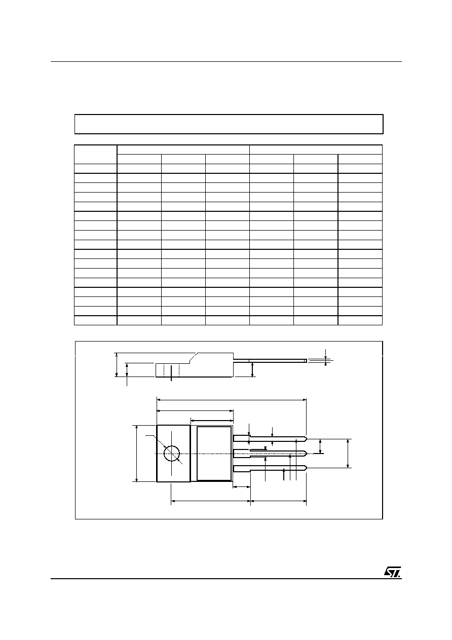
DIM.
mm.
inch
MIN.
TYP
MAX.
MIN.
TYP.
MAX.
A
4.4
4.6
0.173
0.181
B
2.5
2.7
0.098
0.106
D
2.5
2.75
0.098
0.108
E
0.45
0.7
0.017
0.027
F
0.75
1
0.030
0.039
F1
1.15
1.7
0.045
0.067
F2
1.15
1.7
0.045
0.067
G
4.95
5.2
0.195
0.204
G1
2.4
2.7
0.094
0.106
H
10
10.4
0.393
0.409
L2
16
0.630
L3
28.6
30.6
1.126
1.204
L4
9.8
10.6
.0385
0.417
L5
2.9
3.6
0.114
0.141
L6
15.9
16.4
0.626
0.645
L7
9
9.3
0.354
0.366
ÿ
3
3.2
0.118
0.126
TO-220FP MECHANICAL DATA

9/9
STP80NF10/STP80NF10FP
Information furnished is believed to be accurate and reliable. However, STMicroelectronics assumes no responsibility for the
consequences of use of such information nor for any infringement of patents or other rights of third parties which may result from
its use. No license is granted by implication or otherwise under any patent or patent rights of STMicroelectronics. Specifications
mentioned in this publication are subject to change without notice. This publication supersedes and replaces all information
previously supplied. STMicroelectronics products are not authorized for use as critical components in life support devices or
systems without express written approval of STMicroelectronics.
© The ST logo is a registered trademark of STMicroelectronics
© 2002 STMicroelectronics - Printed in Italy - All Rights Reserved
STMicroelectronics GROUP OF COMPANIES
Australia - Brazil - Canada - China - Finland - France - Germany - Hong Kong - India - Israel - Italy - Japan - Malaysia - Malta - Morocco
Singapore - Spain - Sweden - Switzerland - United Kingdom - United States.
© http://www.st.com