1/6
PRELIMINARY DATA
May 2003
This is preliminary information on a new product now in development or undergoing evaluation. Details are subject to change without notice.
STP80NS04ZB
N-CHANNEL CLAMPED 7.5m
- 80A TO-220
FULLY PROTECTED MESH OVERLAYTM MOSFET
s
TYPICAL R
DS
(on) = 0.0075
s
100% AVALANCHE TESTED
s
LOW CAPACITANCE AND GATE CHARGE
s
175
o
C MAXIMUM JUNCTION
TEMPERATURE
DESCRIPTION
This fully clamped Mosfet is produced by using the latest
advanced Company's Mesh Overlay process which is
based on a novel strip layout.
The inherent benefits of the new technology coupled with
the extra clamping capabilities make this product
particularly suitable for the harshest operation conditions
such as those encountered in the automotive
environment. Any other application requiring extra
ruggedness is also recommended.
APPLICATIONS
s
ABS, SOLENOID DRIVERS
s
MOTOR CONTROL
s
DC-DC CONVERTERS
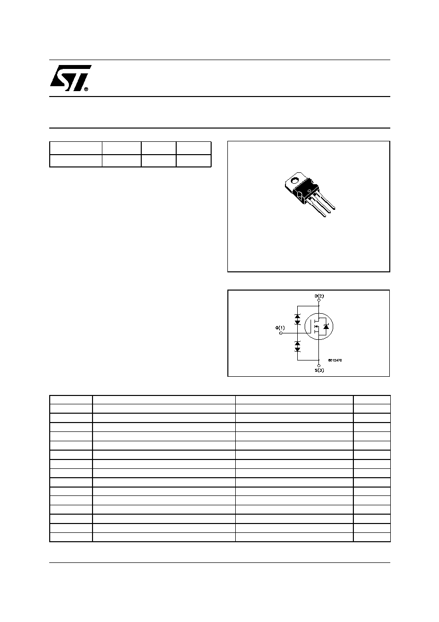
TYPE
V
DSS
R
DS(on)
I
D
STP80NS04ZB
CLAMPED
<0.008
80 A
1
2
3
TO-220
ABSOLUTE MAXIMUM RATINGS
(
�)
Pulse width limited by safe operating area.
Symbol
Parameter
Value
Unit
V
DS
Drain-source Voltage (V
GS
= 0)
CLAMPED
V
V
DG
Drain-gate Voltage
CLAMPED
V
V
GS
Gate- source Voltage
CLAMPED
V
I
D
Drain Current (continuous) at T
C
= 25�C
80
A
I
D
Drain Current (continuous) at T
C
= 100�C
60
A
I
DG
Drain Gate Current (continuous)
� 50
mA
I
GS
Gate SourceCurrent (continuous)
� 50
mA
I
DM
(
�)
Drain Current (pulsed)
320
A
P
tot
Total Dissipation at T
C
= 25�C
200
W
Derating Factor
1.33
W/�C
V
ESD(G-S)
Gate-Source ESD (HBM - C = 100pF, R=1.5 k
)
4
kV
V
ESD(G-D)
Gate-Drain ESD (HBM - C = 100pF, R=1.5 k
)
4
kV
V
ESD(D-S)
Drain-source ESD (HBM - C = 100pF, R=1.5 k
)
4
kV
T
stg
Storage Temperature
-65 to 175
�C
T
j
Max. Operating Junction Temperature
-40 to 175
�C
INTERNAL SCHEMATIC DIAGRAM
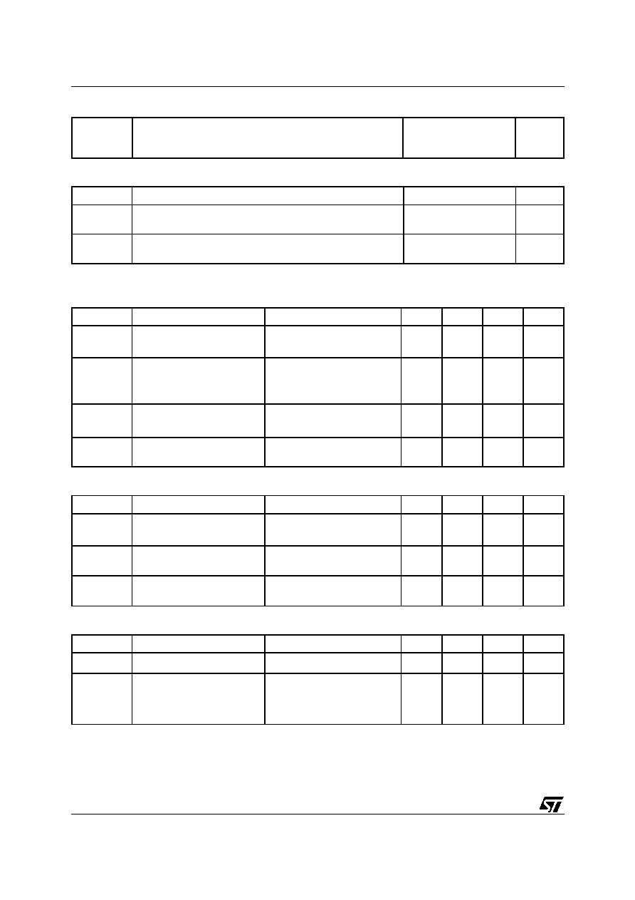
STP80NS04ZB
2/6
THERMAL DATA
AVALANCHE CHARACTERISTICS
ELECTRICAL CHARACTERISTICS (T
case
= 25 �C unless otherwise specified)
OFF
ON
(*)
DYNAMIC
Rthj-case
Rthj-amb
T
l
Thermal Resistance Junction-case
Thermal Resistance Junction-ambient
Maximum Lead Temperature For Soldering Purpose
Max
Max
0.75
62.5
300
�C/W
�C/W
�C
Symbol
Parameter
Max Value
Unit
I
AR
Avalanche Current, Repetitive or Not-Repetitive
(pulse width limited by T
j
max)
80
A
E
AS
Single Pulse Avalanche Energy
(starting T
j
= 25 �C, I
D
= I
AR
, V
DD
= 30 V)
500
mJ
Symbol
Parameter
Test Conditions
Min.
Typ.
Max.
Unit
V
(BR)DSS
Clamped Voltage
I
D
= 1 mA,
V
GS
= 0
-40 < T
J
< 175
o
C
33
V
I
DSS
Zero Gate Voltage
Drain Current (V
GS
= 0)
V
DS
= 16 V
T
c
=25
o
C
V
DS
= 16 V
T
J
=150
o
C
V
DS
= 16 V
T
J
=175
o
C
10
50
100
�A
�A
�A
I
GSS
Gate-body Leakage
Current (V
DS
= 0)
V
GS
= � 10 V
T
J
=175
o
C
V
GS
= � 16 V
T
J
=175
o
C
50
150
�A
�A
V
GSS
Gate-Source
Breakdown Voltage
I
GS
= 100 �A
18
V
Symbol
Parameter
Test Conditions
Min.
Typ.
Max.
Unit
V
GS(th)
Gate Threshold Voltage
V
DS
= V
GS
I
D
= 1 mA
-40 < T
J
< 150
o
C
1.7
3
4.2
V
R
DS(on)
Static Drain-source On
Resistance
V
GS
= 10 V
I
D
= 40 A
V
GS
= 16 V
I
D
= 40 A
8
7.5
9
8
m
m
I
D(on)
On State Drain Current
V
DS
> I
D(on)
x R
DS(on)max,
V
GS
= 10V
80
A
Symbol
Parameter
Test Conditions
Min.
Typ.
Max.
Unit
g
fs
(*)
Forward Transconductance
V
DS
>I
D(on)
xR
DS(on)max
I
D
=40A
30
50
S
C
iss
C
oss
C
rss
Input Capacitance
Output Capacitance
Reverse Transfer
Capacitance
V
DS
= 25V, f = 1 MHz, V
GS
= 0
2700
1275
285
3300
1600
350
pF
pF
pF
3/6
STP80NS04ZB
SWITCHING ON
SWITCHING OFF
SOURCE DRAIN DIODE
(*)
Pulsed: Pulse duration = 300 �s, duty cycle 1.5 %.
(
�)
Pulse width limited by safe operating area.
Symbol
Parameter
Test Conditions
Min.
Typ.
Max.
Unit
Q
g
Q
gs
Q
gd
Total Gate Charge
Gate-Source Charge
Gate-Drain Charge
V
DD
= 20 V I
D
= 80 A V
GS
= 10V
80
20
27
105
nC
nC
nC
Symbol
Parameter
Test Conditions
Min.
Typ.
Max.
Unit
t
r(Voff)
t
f
t
c
Off-voltage Rise Time
Fall Time
Cross-over Time
V
clamp
= 30 V
I
D
= 80 A
R
G
= 4.7
,
V
GS
= 10 V
(Inductive Load, Figure 5)
115
80
210
150
105
280
ns
ns
ns
Symbol
Parameter
Test Conditions
Min.
Typ.
Max.
Unit
I
SD
I
SDM
(
�)
Source-drain Current
Source-drain Current (pulsed)
80
320
A
A
V
SD
(*)
Forward On Voltage
I
SD
= 80 A
V
GS
= 0
1.5
V
t
rr
Q
rr
I
RRM
Reverse Recovery Time
Reverse Recovery Charge
Reverse Recovery Current
I
SD
= 80 A
di/dt = 100A/�s
V
DD
= 25 V
T
j
= 150�C
(see test circuit, Figure 5)
90
0.18
4
ns
�
C
A
ELECTRICAL CHARACTERISTICS (continued)
STP80NS04ZB
4/6
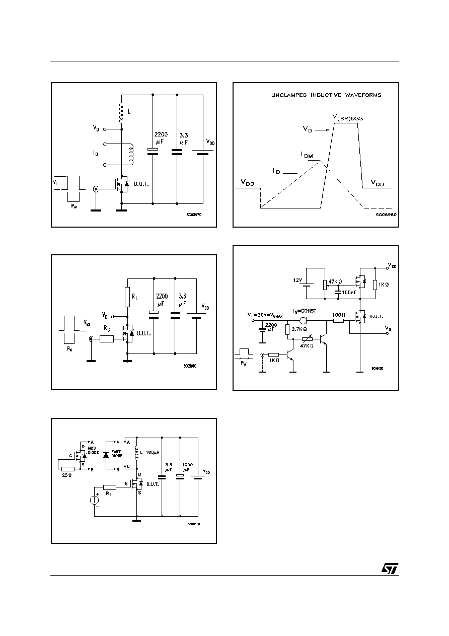
Fig. 1: Unclamped Inductive Load Test Circuit
Fig. 1: Unclamped Inductive Load Test Circuit
Fig. 2: Unclamped Inductive Waveform
Fig. 3: Switching Times Test Circuits For Resistive
Load
Fig. 4: Gate Charge test Circuit
Fig. 5: Test Circuit For Inductive Load Switching
And Diode Recovery Times

5/6
STP80NS04ZB
DIM.
mm
inch
MIN.
TYP.
MAX.
MIN.
TYP.
MAX.
A
4.40
4.60
0.173
0.181
C
1.23
1.32
0.048
0.051
D
2.40
2.72
0.094
0.107
D1
1.27
0.050
E
0.49
0.70
0.019
0.027
F
0.61
0.88
0.024
0.034
F1
1.14
1.70
0.044
0.067
F2
1.14
1.70
0.044
0.067
G
4.95
5.15
0.194
0.203
G1
2.4
2.7
0.094
0.106
H2
10.0
10.40
0.393
0.409
L2
16.4
0.645
L4
13.0
14.0
0.511
0.551
L5
2.65
2.95
0.104
0.116
L6
15.25
15.75
0.600
0.620
L7
6.2
6.6
0.244
0.260
L9
3.5
3.93
0.137
0.154
DIA.
3.75
3.85
0.147
0.151
L6
A
C
D
E
D1
F
G
L7
L2
Dia.
F1
L5
L4
H2
L9
F2
G1
TO-220 MECHANICAL DATA
P011C