1/9
April 2001
STP8NS25
STP8NS25FP
N-CHANNEL 250V - 0.38
- 8A TO-220/TO-220FP
MESH OVERLAYTM MOSFET
s
TYPICAL R
DS
(on) = 0.38
s
EXTREMELY HIGH dv/dt CAPABILITY
s
100% AVALANCHE TESTED
DESCRIPTION
Using the latest high voltage MESH OVERLAYTM
process, STMicroelectronics has designed an ad-
vanced family of power MOSFETs with outstanding
performance. The new patented STrip layout cou-
pled with the Company's proprietary edge termina-
tion structure, makes it suitable in coverters for
lighting applications.
APPLICATIONS
s
HIGH CURRENT, HIGH SPEED SWITCHING
s
SWITH MODE POWER SUPPLIES (SMPS)
s
DC-DC CONVERTERS FOR TELECOM,
INDUSTRIAL, AND LIGHTING EQUIPMENT
ABSOLUTE MAXIMUM RATINGS
(∑)Pulse width limited by safe operating area
TYPE
V
DSS
R
DS(on)
I
D
STP8NS25
STP8NS25FP
250 V
250 V
< 0.45
< 0.45
8 A
8 A
Symbol
Parameter
Value
Unit
STP8NS25
STP8NS25FP
V
DS
Drain-source Voltage (V
GS
= 0)
250
V
V
DGR
Drain-gate Voltage (R
GS
= 20 k
)
250
V
V
GS
Gate- source Voltage
± 20
V
I
D
Drain Current (continuos) at T
C
= 25∞C
8
8(*)
A
I
D
Drain Current (continuos) at T
C
= 100∞C
5
5(*)
A
I
DM
(
q
)
Drain Current (pulsed)
32
32(*)
A
P
TOT
Total Dissipation at T
C
= 25∞C
80
30
W
Derating Factor
0.64
0.24
W/∞C
dv/dt (1)
Peak Diode Recovery voltage slope
5
V/ns
V
ISO
Insulation Withstand Voltage (DC)
-
2000
V
T
stg
Storage Temperature
≠65 to 150
∞C
T
j
Max. Operating Junction Temperature
150
∞C
(1) I
SD
8A, di/dt
300 A/
µ
s, V
DD
V
(BR)DSS
, Tj
T
jMAX
(*)Limited only by maximum temperature allowed
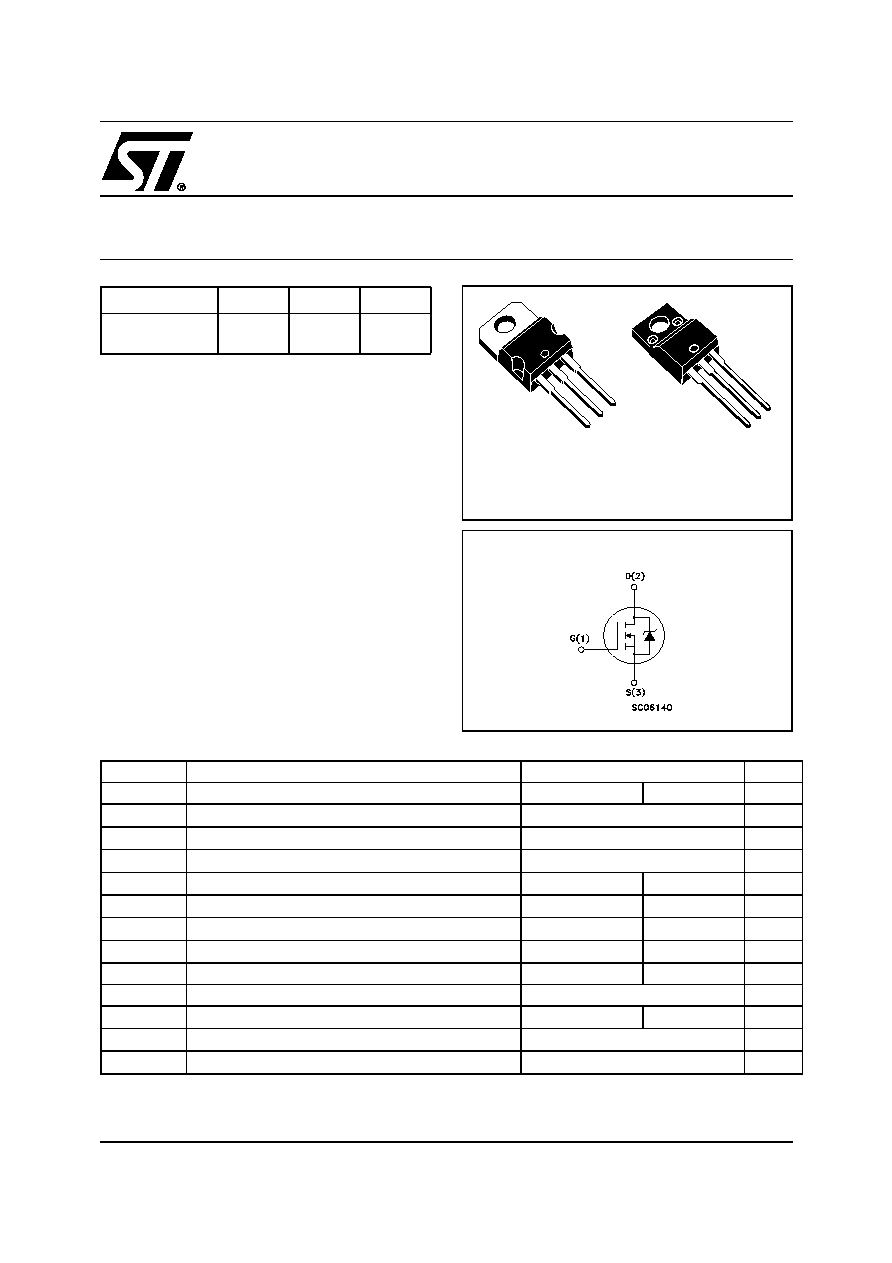
INTERNAL SCHEMATIC DIAGRAM
TO-220
1
2
3
1
2
3
TO-220FP
STP8NS25/STP8NS25FP
2/9
THERMAL DATA
ELECTRICAL CHARACTERISTICS (TCASE = 25 ∞C UNLESS OTHERWISE SPECIFIED)
OFF
ON
(1)
DYNAMIC
TO-220
TO-220FP
Rthj-case
Thermal Resistance Junction-case Max
1.56
4.11
∞C/W
Rthj-amb
Thermal Resistance Junction-ambient Max
62.5
∞C/W
Rthc-sink
Thermal Resistance Case-sink Typ
0.5
∞C/W
T
l
Maximum Lead Temperature For Soldering Purpose
300
∞C
Symbol
Parameter
Test Conditions
Min.
Typ.
Max.
Unit
V
(BR)DSS
Drain-source
Breakdown Voltage
I
D
= 250 µA, V
GS
= 0
250
V
I
DSS
Zero Gate Voltage
Drain Current (V
GS
= 0)
V
DS
= Max Rating
1
µA
V
DS
= Max Rating, T
C
= 125 ∞C
10
µA
I
GSS
Gate-body Leakage
Current (V
DS
= 0)
V
GS
= ±20V
±100
nA
Symbol
Parameter
Test Conditions
Min.
Typ.
Max.
Unit
V
GS(th)
Gate Threshold Voltage
V
DS
= V
GS
, I
D
= 250µA
2
3
4
V
R
DS(on)
Static Drain-source On
Resistance
V
GS
= 10V, I
D
= 4 A
0.38
0.45
I
D(on)
On State Drain Current
V
DS
> I
D(on)
x R
DS(on)max,
V
GS
= 10V
8
A
Symbol
Parameter
Test Conditions
Min.
Typ.
Max.
Unit
g
fs
(1)
Forward Transconductance
V
DS
> I
D(on)
x R
DS(on)max,
I
D
= 4A
7
8
S
C
iss
Input Capacitance
V
DS
= 25V, f = 1 MHz, V
GS
= 0
770
pF
C
oss
Output Capacitance
118
pF
C
rss
Reverse Transfer
Capacitance
48
pF
3/9
STP8NS25/STP8NS25FP
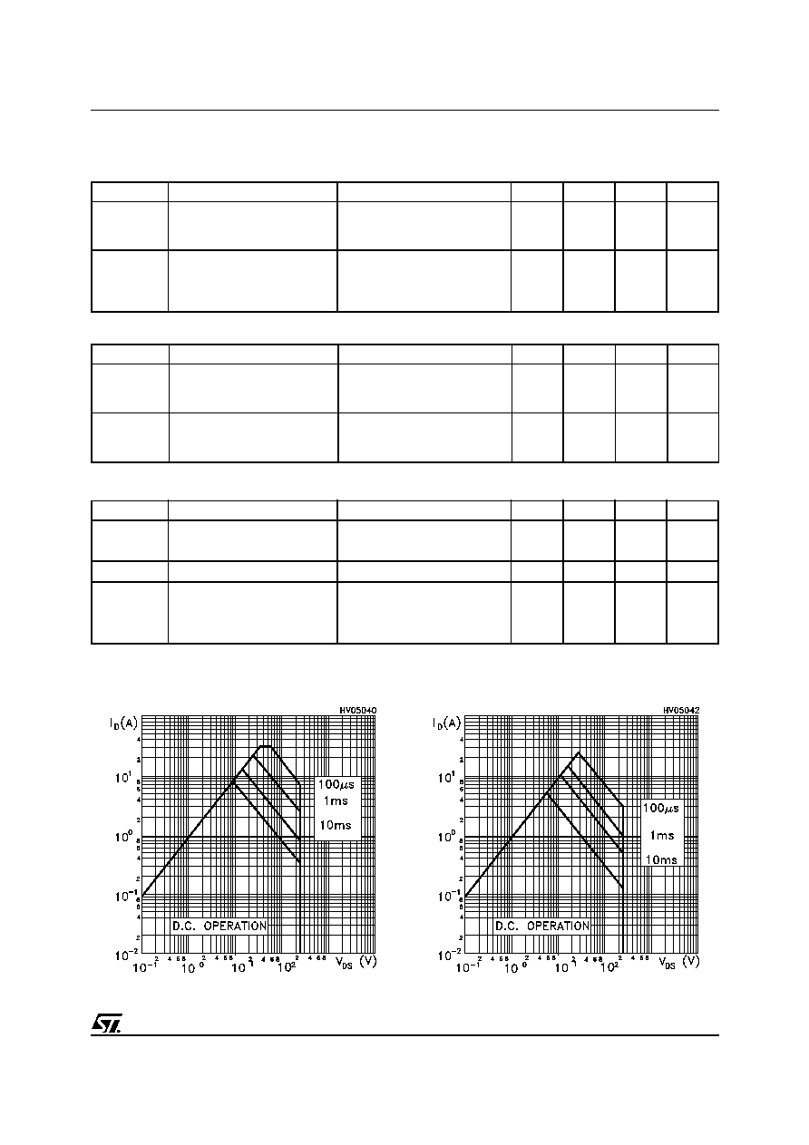
Safe Operating Area for TO-220
ELECTRICAL CHARACTERISTICS (CONTINUED)
SWITCHING ON
SWITCHING OFF
SOURCE DRAIN DIODE
Note: 1. Pulsed: Pulse duration = 300 µs, duty cycle 1.5 %.
2. Pulse width limited by safe operating area.
Symbol
Parameter
Test Conditions
Min.
Typ.
Max.
Unit
t
d(on)
Turn-on Delay Time
V
DD
= 125 V, I
D
= 4 A
R
G
= 4.7
V
GS
= 10 V
(see test circuit, Figure 3)
13
ns
t
r
Rise Time
18
ns
Q
g
Total Gate Charge
V
DD
= 200V, I
D
= 8 A,
V
GS
= 10V
37
51.8
nC
Q
gs
Gate-Source Charge
5.2
nC
Q
gd
Gate-Drain Charge
14.8
nC
Symbol
Parameter
Test Conditions
Min.
Typ.
Max.
Unit
t
d(Voff)
t
f
Turn-off- Delay Time
Fall Time
V
DD
= 125V, I
D
= 4 A,
R
G
= 4.7
,
V
GS
= 10V
(see test circuit, Figure 3)
51
16
ns
ns
t
r(Voff)
t
f
t
c
Off-voltage Rise Time
Fall Time
Cross-over Time
V
clamp
= 200V, I
D
= 8 A,
R
G
= 4.7
,
V
GS
= 10V
(see test circuit, Figure 5)
12.5
12.5
28
ns
ns
ns
Symbol
Parameter
Test Conditions
Min.
Typ.
Max.
Unit
I
SD
Source-drain Current
8
A
I
SDM
(2)
Source-drain Current (pulsed)
32
A
V
SD
(1)
Forward On Voltage
I
SD
= 8 A, V
GS
= 0
1.7
V
t
rr
Reverse Recovery Time
I
SD
= 8 A, di/dt = 100A/µs
V
DD
= 30V, T
j
= 150∞C
(see test circuit, Figure 5)
198
ns
Q
rr
Reverse Recovery Charge
1.1
µ
C
I
RRM
Reverse Recovery Current
11.3
A
Safe Operating Area for TO-220FP
STP8NS25/STP8NS25FP
4/9
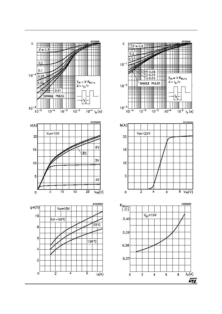
Thermal Impedence for TO-220FP
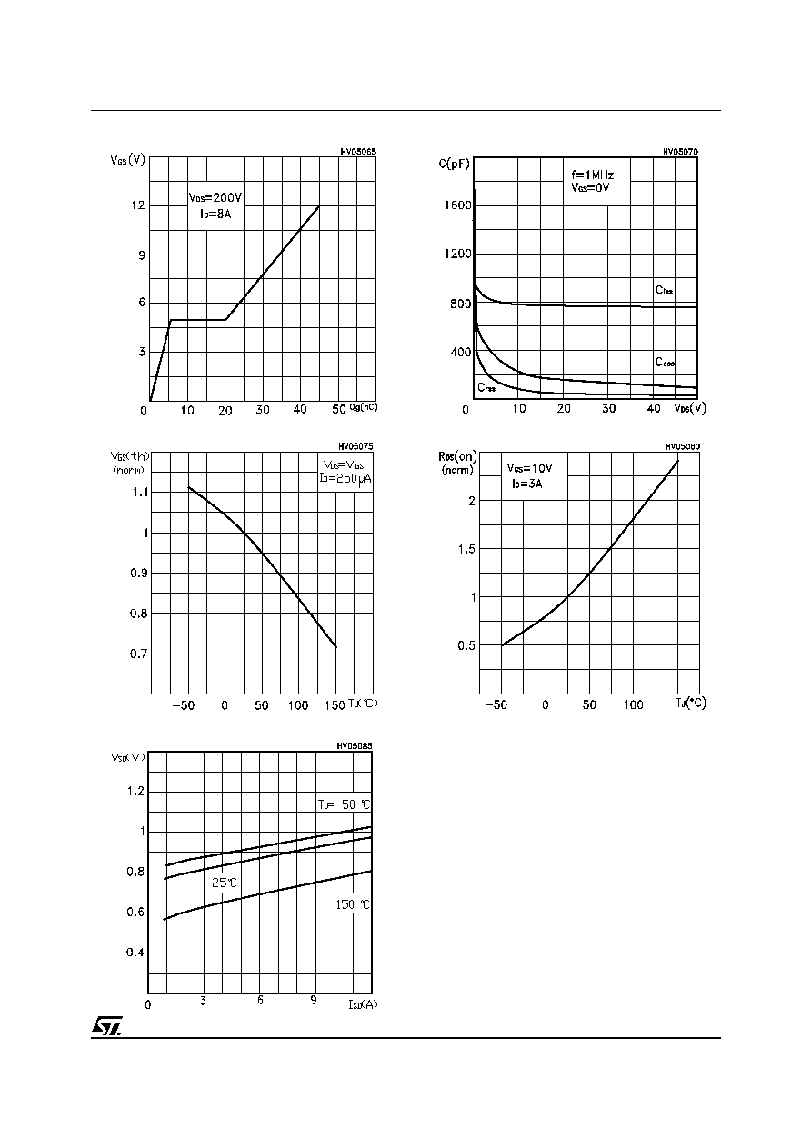
Static Drain-source On Resistance
Transconductance
Output Characteristics
Transfer Characteristics
Thermal Impedence for TO-220
5/9
STP8NS25/STP8NS25FP
Source-drain Diode Forward Characteristics
Normalized On Resistance vs Temperature
Normalized Gate Thereshold Voltage vs Temp.
Gate Charge vs Gate-source Voltage
Capacitance Variations
STP8NS25/STP8NS25FP
6/9
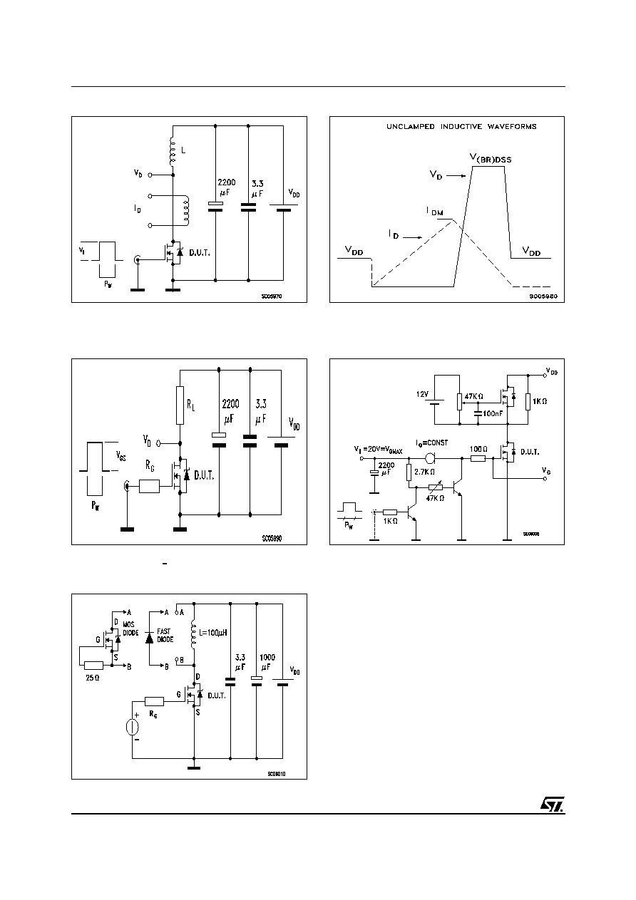
Fig. 5: Test Circuit For Inductive Load Switching
And Diode Recovery Times
Fig. 4: Gate Charge test Circuit
Fig. 2: Unclamped Inductive Waveform
Fig. 1: Unclamped Inductive Load Test Circuit
Fig. 3: Switching Times Test Circuit For
Resistive Load
7/9
STP8NS25/STP8NS25FP
DIM.
mm
inch
MIN.
TYP.
MAX.
MIN.
TYP.
MAX.
A
4.40
4.60
0.173
0.181
C
1.23
1.32
0.048
0.051
D
2.40
2.72
0.094
0.107
D1
1.27
0.050
E
0.49
0.70
0.019
0.027
F
0.61
0.88
0.024
0.034
F1
1.14
1.70
0.044
0.067
F2
1.14
1.70
0.044
0.067
G
4.95
5.15
0.194
0.203
G1
2.4
2.7
0.094
0.106
H2
10.0
10.40
0.393
0.409
L2
16.4
0.645
L4
13.0
14.0
0.511
0.551
L5
2.65
2.95
0.104
0.116
L6
15.25
15.75
0.600
0.620
L7
6.2
6.6
0.244
0.260
L9
3.5
3.93
0.137
0.154
DIA.
3.75
3.85
0.147
0.151
L6
A
C
D
E
D1
F
G
L7
L2
Dia.
F1
L5
L4
H2
L9
F2
G1
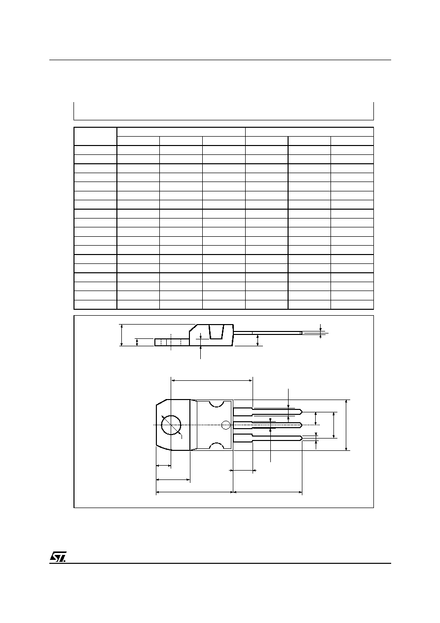
TO-220 MECHANICAL DATA
P011C
STP8NS25/STP8NS25FP
8/9
DIM.
mm
inch
MIN.
TYP.
MAX.
MIN.
TYP.
MAX.
A
4.4
4.6
0.173
0.181
B
2.5
2.7
0.098
0.106
D
2.5
2.75
0.098
0.108
E
0.45
0.7
0.017
0.027
F
0.75
1
0.030
0.039
F1
1.15
1.7
0.045
0.067
F2
1.15
1.7
0.045
0.067
G
4.95
5.2
0.195
0.204
G1
2.4
2.7
0.094
0.106
H
10
10.4
0.393
0.409
L2
16
0.630
L3
28.6
30.6
1.126
1.204
L4
9.8
10.6
0.385
0.417
L6
15.9
16.4
0.626
0.645
L7
9
9.3
0.354
0.366
ÿ
3
3.2
0.118
0.126
L2
A
B
D
E
H
G
L6
Ø
F
L3
G1
1 2 3
F2
F1
L7
L4
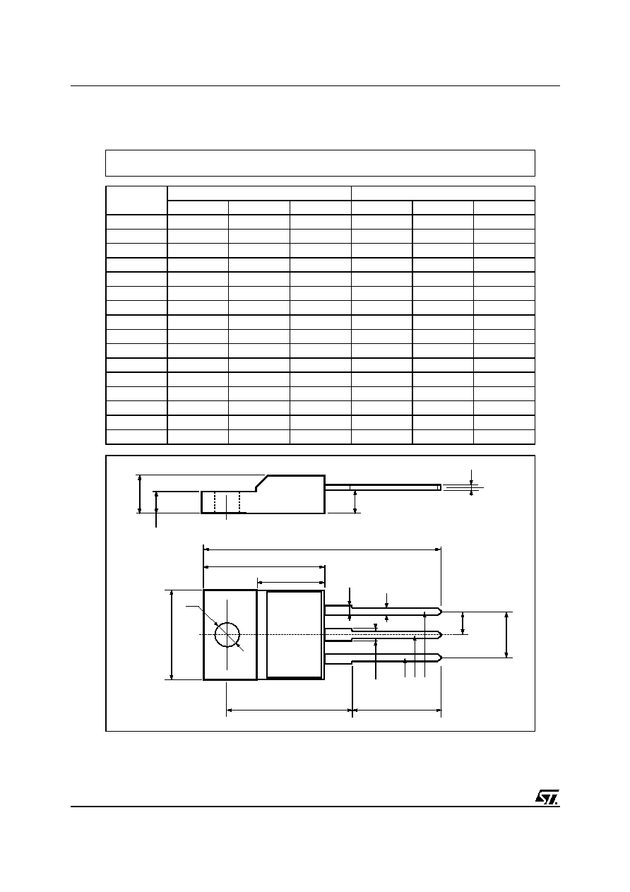
TO-220FP MECHANICAL DATA

9/9
STP8NS25/STP8NS25FP
Information furnished is believed to be accurate and reliable. However, STMicroelectronics assumes no responsibility for the consequences
of use of such information nor for any infringement of patents or other rights of third parties which may result from its use. No license is
granted by implication or otherwise under any patent or patent rights of STMicroelectronics. Specification mentioned in this publication are
subject to change without notice. This publication supersedes and replaces all information previously supplied. STMicroelectronics products
are not authorized for use as critical components in life support devices or systems without express written approval of STMicroelectronics.
The ST logo is a trademark of STMicroelectronics
© 2001 STMicroelectronics ≠ Printed in Italy ≠ All Rights Reserved
STMicroelectronics GROUP OF COMPANIES
Australia - Brazil - China - Finland - France - Germany - Hong Kong - India - Italy - Japan - Malaysia - Malta - Morocco -
Singapore - Spain - Sweden - Switzerland - United Kingdom - U.S.A.
http://www.st.com