1/9
April 2003
STP90NF03L
STB90NF03L-1
N-CHANNEL 30V - 0.0056
- 90A TO-220/I
2
PAK
LOW GATE CHARGE STripFETTM POWER MOSFET
s
TYPICAL R
DS
(on) = 0.0056
s
TYPICAL Q
g
= 35 nC @ 5V
s
OPTIMAL R
DS
(on) x Q
g
TRADE-OFF
s
CONDUCTION LOSSES REDUCED
s
SWITCHING LOSSES REDUCED
DESCRIPTION
This application specific Power Mosfet is the third
generation of STMicroelectronics unique "Single
Feature Size
TM"
strip-based process. The resulting
transistor shows the best trade-off between on-re-
sistance and gate charge. When used as high and
low side in buck regulators, it gives the best perfor-
mance in terms of both conduction and switching
losses. This is extremely important for mother-
boards where fast switching and high efficiency are
of paramount importance.
APPLICATIONS
s
SPECIFICALLY DESIGNED AND OPTIMISED
FOR HIGH EFFICIENCY CPU CORE DC/DC
CONVERTERS
ORDERING INFORMATION
TYPE
V
DSS
R
DS(on)
I
D
STP90NF03L
STB90NF03L-1
30 V
30 V
< 0.0065
< 0.0065
90 A
90 A
SALES TYPE
MARKING
PACKAGE
PACKAGING
STP90NF03L
P90NF03L
TO-220
TUBE
STB90NF03L-1
B90NF03L
I
2
PAK
TUBE
TO-220
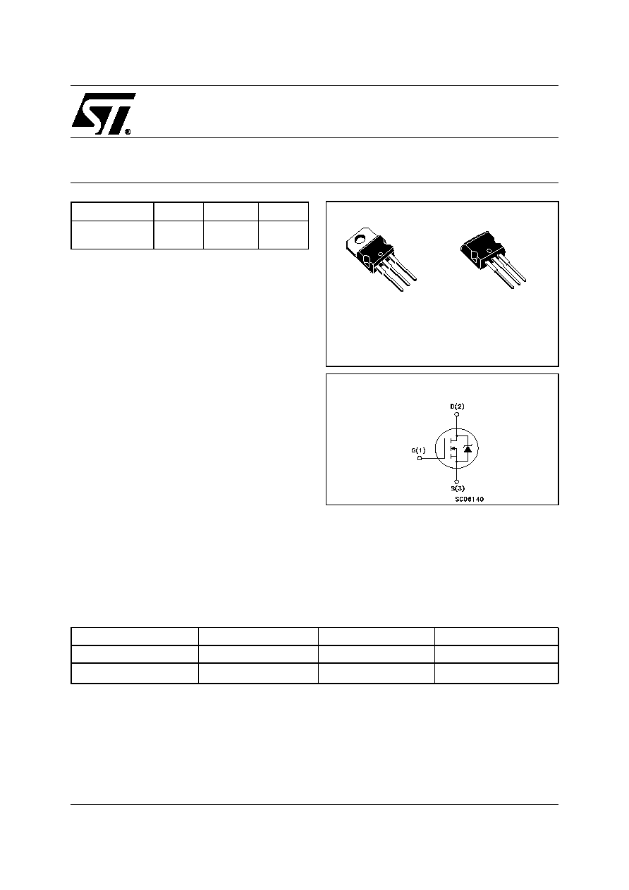
1
2
3
1
2
3
I
2
PAK
INTERNAL SCHEMATIC DIAGRAM
STP90NF03L/STB90NF03L-1
2/9
ABSOLUTE MAXIMUM RATINGS
( ) Pulse width limited by safe operating area
THERMAL DATA
ELECTRICAL CHARACTERISTICS (T
CASE
= 25 ∞C UNLESS OTHERWISE SPECIFIED)
ON /OFF
Symbol
Parameter
Value
Unit
V
DS
Drain-source Voltage (V
GS
= 0)
30
V
V
DGR
Drain-gate Voltage (R
GS
= 20 k
)
30
V
V
GS
Gate- source Voltage
±20
V
I
D
Drain Current (continuous) at T
C
= 25∞C
90
A
I
D
Drain Current (continuous) at T
C
= 100∞C
65
A
I
DM
( )
Drain Current (pulsed)
360
A
P
TOT
Total Dissipation at T
C
= 25∞C
150
W
Derating Factor
0.73
W/∞C
T
stg
Storage Temperature
≠65 to 175
∞C
T
j
Max. Operating Junction Temperature
175
∞C
Rthj-case
Thermal Resistance Junction-case Max
1
∞C/W
Rthj-amb
Thermal Resistance Junction-ambient Max
62.5
∞C/W
T
l
Maximum Lead Temperature For Soldering Purpose
300
∞C
Symbol
Parameter
Test Conditions
Min.
Typ.
Max.
Unit
V
(BR)DSS
Drain-source
Breakdown Voltage
I
D
= 250 µA, V
GS
= 0
30
V
I
DSS
Zero Gate Voltage
Drain Current (V
GS
= 0)
V
DS
= Max Rating
1
µA
V
DS
= Max Rating, T
C
= 125 ∞C
10
µA
I
GSS
Gate-body Leakage
Current (V
DS
= 0)
V
GS
= ±20V
±100
nA
I
D(on)
On State Drain Current
V
DS
> I
D(on)
x R
DS(on)max,
V
GS
= 10V
90
A
V
GS(th)
Gate Threshold Voltage
V
DS
= V
GS
, I
D
= 250 µA
1
2.5
V
R
DS(on)
Static Drain-source On
Resistance
V
GS
= 10V, I
D
= 45 A
0.0056
0.0065
V
GS
= 5V, I
D
= 45 A
0.007
0.012

3/9
STP90NF03L/STB90NF03L-1
ELECTRICAL CHARACTERISTICS (CONTINUED)
DYNAMIC
SWITCHING ON
SWITCHING OFF
SOURCE DRAIN DIODE
Note: 1. Pulsed: Pulse duration = 300 µs, duty cycle 1.5 %.
2. Pulse width limited by safe operating area.
Symbol
Parameter
Test Conditions
Min.
Typ.
Max.
Unit
g
fs
(1)
Forward Transconductance
V
DS
> I
D(on)
x R
DS(on)max,
I
D
= 45 A
40
S
C
iss
Input Capacitance
V
DS
= 25V, f = 1 MHz, V
GS
= 0
2700
pF
C
oss
Output Capacitance
860
pF
C
rss
Reverse Transfer Capacitance
170
pF
Symbol
Parameter
Test Conditions
Min.
Typ.
Max.
Unit
t
d(on)
Turn-on Delay Time
V
DD
= 15V, I
D
= 45 A
R
G
= 4.7
V
GS
= 4.5 V
(see test circuit, Figure 3)
30
ns
t
r
Rise Time
200
ns
Q
g
Total Gate Charge
V
DD
= 24V, I
D
= 90 A,V
GS
= 5V
35
47
nC
Q
gs
Gate-Source Charge
10
nC
Q
gd
Gate-Drain Charge
18
nC
Symbol
Parameter
Test Conditions
Min.
Typ.
Max.
Unit
t
d(off)
t
f
Turn-off-Delay Time
Fall Time
V
DD
= 1 5V, I
D
= 45 A,
R
G
= 4.7
,
V
GS
= 4.5 V
(see test circuit, Figure 3)
50
105
ns
ns
Symbol
Parameter
Test Conditions
Min.
Typ.
Max.
Unit
I
SD
Source-drain Current
90
A
I
SDM
(2)
Source-drain Current (pulsed)
360
A
V
SD
(1)
Forward On Voltage
I
SD
= 90 A, V
GS
= 0
1.3
V
t
rr
Q
rr
I
RRM
Reverse Recovery Time
Reverse Recovery Charge
Reverse Recovery Current
I
SD
= 90 A, di/dt = 100A/µs,
V
DD
= 15V, T
j
= 150∞C
(see test circuit, Figure 5)
80
90
2.5
ns
nC
A
STP90NF03L/STB90NF03L-1
4/9
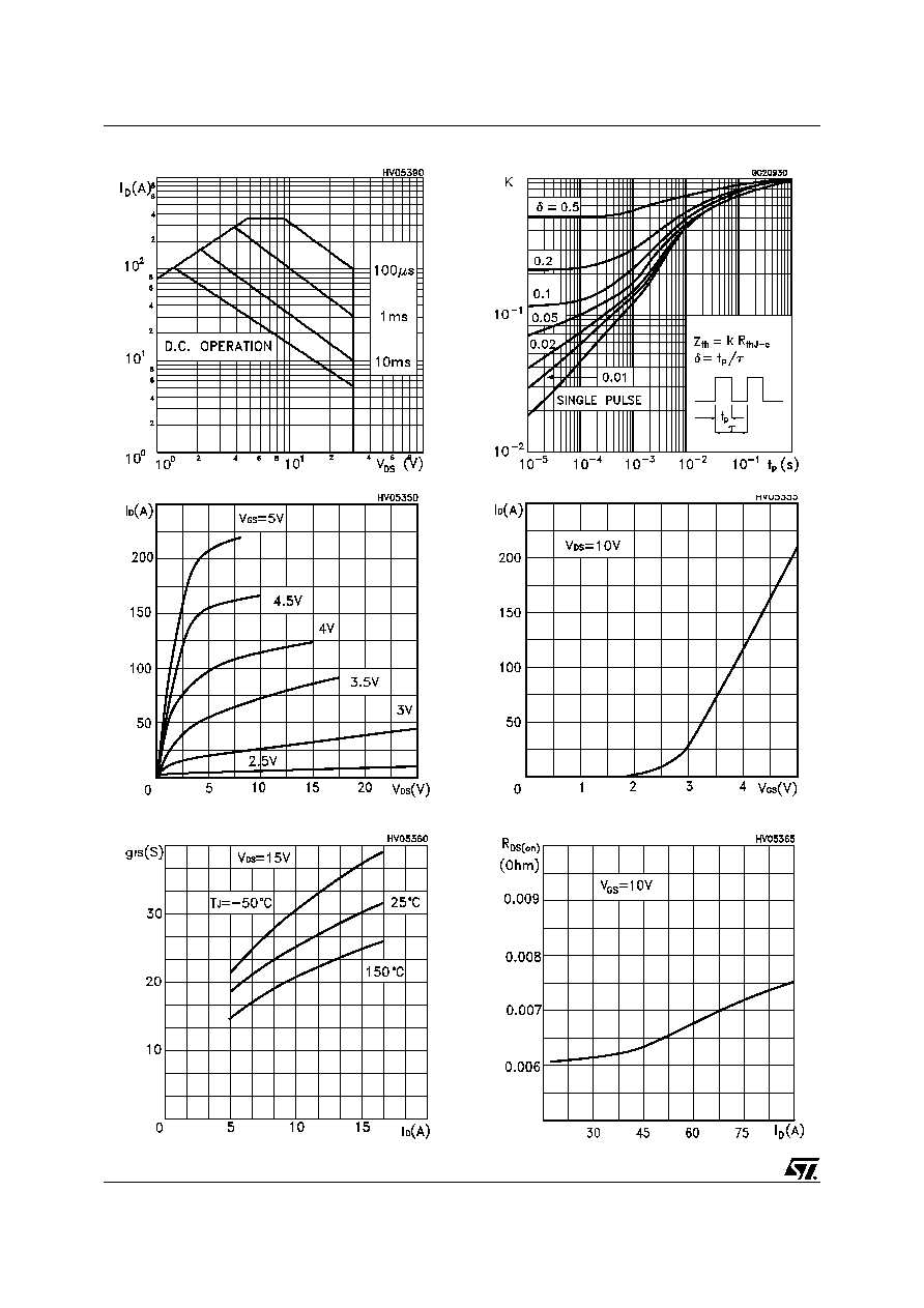
Thermal Impedence
Safe Operating Area
Transconductance
Static Drain-source On Resistance
Output Characteristics
Transfer Characteristics
5/9
STP90NF03L/STB90NF03L-1
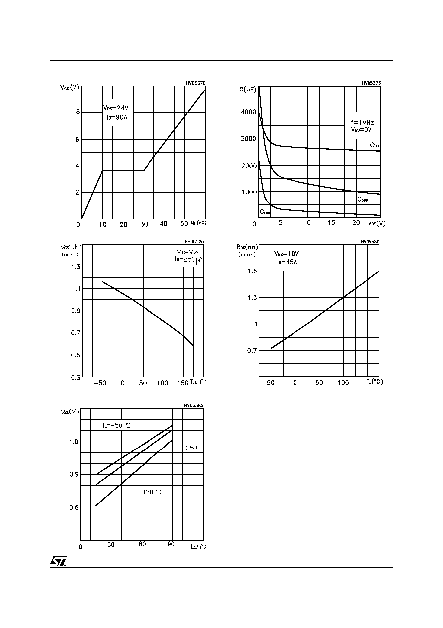
Gate Charge vs Gate-source Voltage
Capacitance Variations
Source-drain Diode Forward Characteristics
Normalized On Resistance vs Temperature
Normalized Gate Thereshold Voltage vs Temp.