 | –≠–ª–µ–∫—Ç—Ä–æ–Ω–Ω—ã–π –∫–æ–º–ø–æ–Ω–µ–Ω—Ç: STPAC01F2 | –°–∫–∞—á–∞—Ç—å:  PDF PDF  ZIP ZIP |

Æ
1/7
MAIN PRODUCT CHARACTERISTICS
The STPAC01F2 has two outputs, one for the sig-
nal detection and another one for the temperature
compensation:
V
DCout
= 0.88 V at 0.85 GHz at 10 dBm
V
DCout
= 1.07 V at 1.85 GHz at 10 dBm
Vsupply = 5 V max
Lead free package
DESCRIPTION
The STPAC01F2 is an integrated RF detector for
the power control stage. It converts RF signal
coming from the coupler into a DC signal usable
by the digital stage. It is based on the use of two
similar diodes, one providing the signal detection
while the second one is used to provide a temper-
ature information to thermal compensation stage.
A biasing stage suppresses the detection diode
drop voltage effect.
Target applications are cellular phones and PDA
using GSM, DCS, PCS, AMPS, TDMA, CDMA and
800 MHz to 1900 MHz frequency ranges.
BENEFITS
The use of IPAD technology allows the RF
front-end designer to save PCB area and to
drastically suppress parasitic inductances.
STPAC01F2
RF DETECTOR FOR
POWER AMPLIFIER CONTROL
REV. 1
October 2004
IPADTM
Flip-Chip
(8 Bumps)
Table 1: Order Code
Part Number
Marking
STPAC01F2
RA
Figure 1: Pin Configuration (Ball side)
Gnd1
RFin
Gnd1
Gnd1
Gnd2
Bias
DC
out
V
Temp
3
2
1
A
B
C
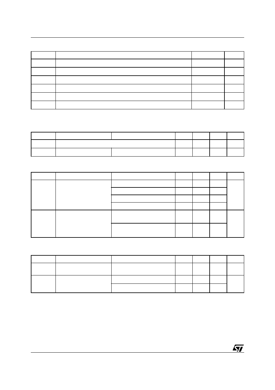
Figure 2: Functional diagram
Coupler
GND2
GND1
V
DCOut
STPAC01F2
RF input
V
BIAS
V
temp
Thermal
compensation
Low pass
filter
RF detector
STPAC01F2
2/7
Table 2: Absolute Retings (T
amb
= 25∞C)
ELECTRICAL CHARACTERISTICS (T
amb
= 25∞C)
Table 3: Parameters related to BIAS voltage
Table 4: Parameters related detection function (V
BIAS
+ 2.7 V, DC output load = 100k
)
Table 5:
Parameters related to detection function
Symbol
Parameter and test conditions
Value
Unit
V
BIAS
Bias voltage
5
V
P
RF
RF power at the RF input
20
dBm
F
OP
Operating frequency range
0.8 to 2
GHz
V
PP
ESD level as per MIL-STD 883E method 3015.7 notice 8 (HBM)
250
V
T
OP
Operating temperature range
- 30 to + 85
∞C
T
STG
Storage temperature range
- 55 to + 150
∞C
Symbol
Parameter
Test conditions
Min.
Typ.
Max.
Unit
V
BIAS
Operating bias voltage
2.2
3.2
V
I
BIAS
Bias current
V
BIAS
= 3.2 V
0.5
mA
Symbol
Parameter
Test conditions
Min.
Typ.
Max.
Unit
V
DCout
DC output voltage
(see fig. 1, I
DC
= 50
µA)
F = 1.85 GHz, P
RF
= 10 dBm
0.97
1.07
1.17
V
F = 1.85 GHz, P
RF
= - 20 dBm
1.83
1.93
2.03
F = 0.85 GHz, P
RF
= 10 dBm
0.78
0.88
0.98
F = 0.85 GHz, P
RF
= - 20 dBm
1.83
1.93
2.03
V
DCout
DC output voltage varia-
tion (see fig. 8,
I
DC
= 50
µA)
0 < T
amb
< 70∞C
F = 1.85 GHz, P
RF
= 10 dBm
0.09
V
2.2 < V
BIAS
< 3.2 V
F = 1.85 GHz, P
RF
= 10 dBm
0.44
Symbol
Parameter
Test conditions
Min.
Typ.
Max.
Unit
V
Temp
Temperature output
voltage (see fig. 9)
I
DC
= 50
µA
1.83
1.93
2.03
V
V
Temp
Temperature output
voltage variation
(see fig. 9)
I
DC
= 50
µA, 0 < T
amb
< 70∞C
0.09
V
I
DC
= 50
µA, 2.2 < V
BIAS
< 3.2V
0.44
STPAC01F2
3/7
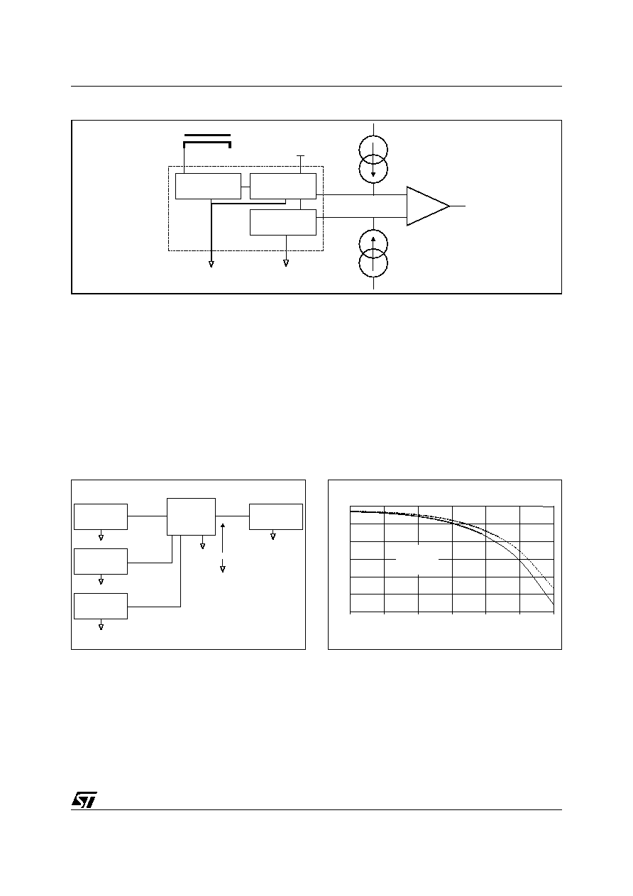
Figure 3: Application diagram
The STPAC01 is the first part of the power amplifier stage and provides both RF power and die tempera-
ture measurements. The above figure gives the basic circuit of RF detector.
A coupler located on the line between RF amplifier output and the antenna takes a part of the available
power and applies it to STPAC01 RF input.
The RF detector and the low pass filter provide a DC voltage depending on the input power. Thermal com-
pensation provides a DC voltage depending on the ambient temperature. As the detection system and the
thermal compensation are based on the same topology, VDCout will have the same temperature variation
as Vtemp. Connected to a differential amplifier, the output will be a voltage directly linked to the RF input
power. VDCout and Vtemp must be bias with 50µA DC current.
This topology offers the most accurate output value as it is 100% compensated.
Coupler
GND2
Out
GND1
V
DCOut
I
DC
= 50µA
I
DC
= 50µA
STPAC01F2
RF input
V
BIAS
V
temp
Thermal
compensation
Low pass
filter
RF detector
-
+
Figure 4: V
DCout
measurement circuit
Figure 5: V
DCout
versus RF input power
V
DCOut
I
DC
RF in
V
BIAS
DC output
voltage
RF generator
Power
supply
Current
generator
STPAC
test board
Multimeter
0.8
1
1.2
1.4
1.6
1.8
2
-20
-15
-10
-5
0
5
10
Pin (dBm)
VDCout
850MHz
1850MHz
Tamb = 25∞C
Ibias = 50µA
Vbias = 2.7V
STPAC01F2
4/7
Figure 6: Relative variation of V
DCout
versus
frequency (from 800 to 900 MHz)
Figure 7: Relative variation of V
DCout
versus
frequency (from 1800 to 1900 MHz)
Figure 8: Temperature effect measurement
circuit on V
DCout
Figure 9: V
temp
measurement circuit
Figure 10: V
temp
output voltage versus
ambient temperature
0.9
0.95
1
1.05
800
825
850
875
900
Frequency in MHz
V
DCout
(Freq.) / V
DCOut
(850MHz)
V
DCout
(Freq.) / V
DCOut
(850MHz)
0.9
0.95
1
1.05
1800
1825
1850
1875
1900
Frequency in MHz
V
DCOut
I
DC
RF in
V
BIAS
DC output
voltage
RF generator
Power
supply
Current
generator
STPAC
test board
Multimeter
Climatic
chamber
V
temp
I
DC
V
BIAS
Temp.
voltage
Power
supply
Current
generator
STPAC
test board
Multimeter
Climatic
chamber
1.88
1.9
1.92
1.94
1.96
1.98
0
10
20
30
40
50
60
70
Tamb (∞C)
Vtemp
Ibias = 50µA
STPAC01F2
5/7
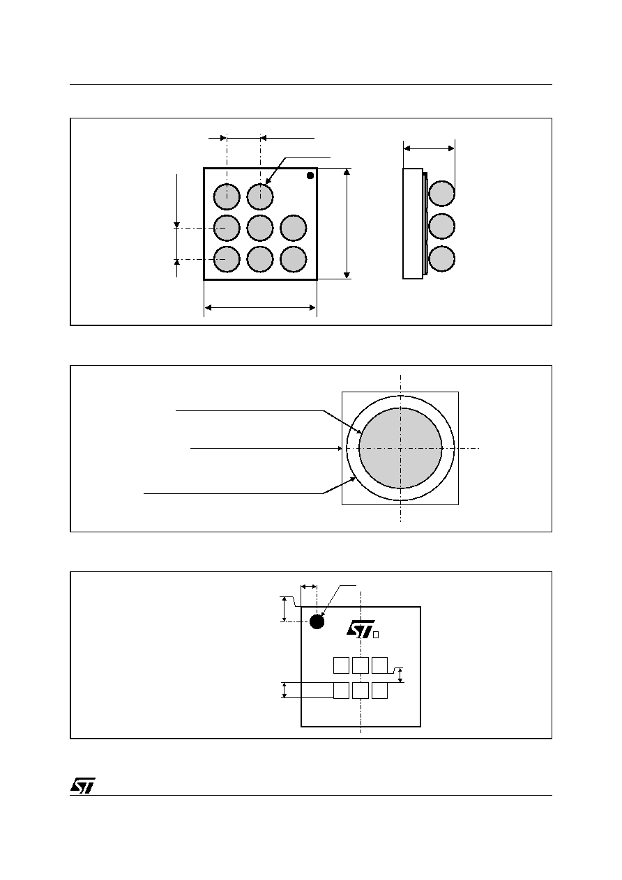
Figure 11: FLIP-CHIP Package Mechanical Data
Figure 12: Foot print recommendations
Figure 13: Marking
1.57mm ± 50µm
1.57mm ± 50µm
315µm ± 50
500µm ± 50
500µm ± 50
650µm ± 65
Copper pad Diameter :
250µm recommended , 300µm max
Solder stencil opening : 330µm
Solder mask opening recommendation :
340µm min for 300µm copper pad diameter
365
365
240
40
220
x
y
x
w
z
w
All dimensions in µm
E
Dot, ST logo
xx = marking
z = packaging location
yww = datecode
(y = year
ww = week)