 | –≠–ª–µ–∫—Ç—Ä–æ–Ω–Ω—ã–π –∫–æ–º–ø–æ–Ω–µ–Ω—Ç: STPAC02F1 | –°–∫–∞—á–∞—Ç—å:  PDF PDF  ZIP ZIP |
1/5
STPAC02F1
Æ
October 2003 - Ed: 1
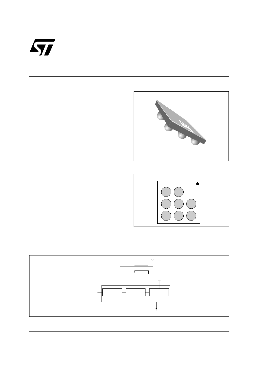
Flip-Chip package
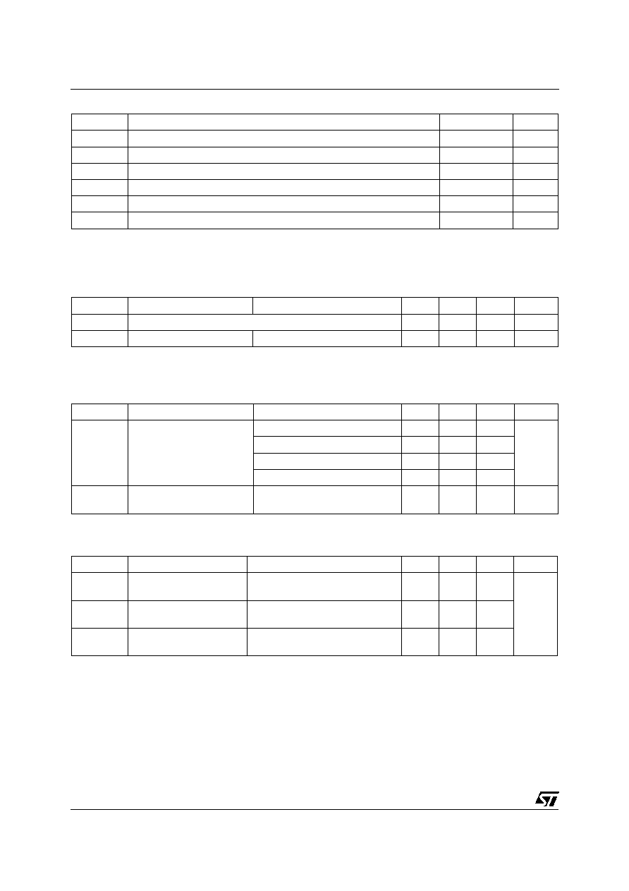
GND
RFin
GND
GND
GND
VBias
OUT
Not
used
3
2
1
A
B
C
PIN CONFIGURATION (ball side)
The use of IPAD technology allows the RF
front-end designer to save PCB area and to
drastically suppress the parasitic inductances.
BENEFITS
RF DETECTOR FOR POWER AMPLIFIER CONTROL
WITH INTERNAL TEMPERATURE COMPENSATION
IPAD
TM
0.8 to 2.5GHz frequency range
Detection diode voltage drop compensation
Temperature compensation
Fast response time
Low Power consumption
Chip Scale device
Low parasitic impedance
MAIN PRODUCT CHARACTERISTICS
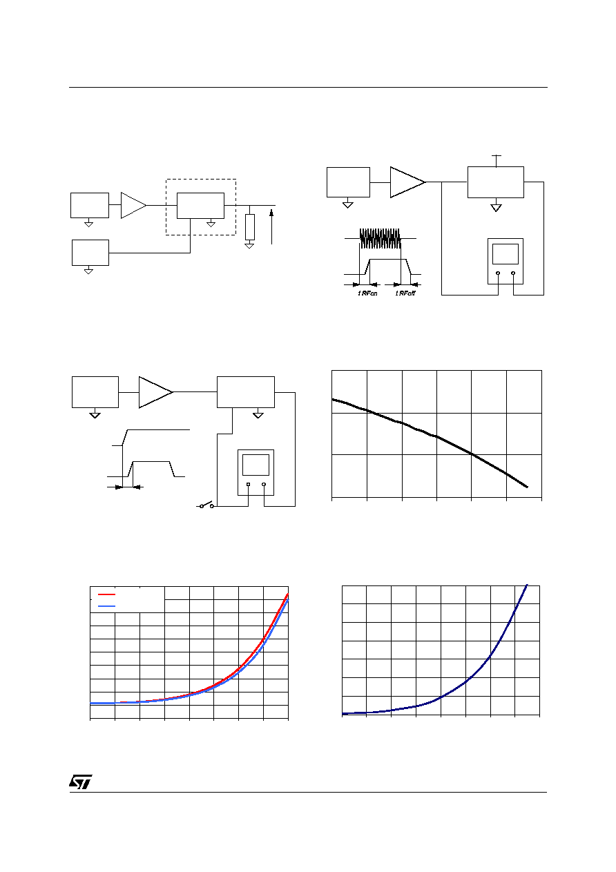
The STPAC02F1 is an integrated RF detector for
power control chain. It has been developed to
convert the RF signal coming from the external
coupler into a DC signal usable by the mobile
digital stage. It is based on the use of two similar
diodes, one assuming the signal detection while
the second one is used to compensate the ambient
temperature effect. A biasing stage suppresses
the detection diode drop voltage effect. The use of
the IPAD technology allows the RF front-end
designer to save PCB area and to drastically
suppress the parasitic inductances of the package.
Target applications are cellular phones and PDA
using GSM, DCS, PCS, AMPS, TDMA , CDMA
and 800MHz to 2100MHz frequency ranges
.
DESCRIPTION
TM : IPAD is a trademark of STMicroelectronics.
Coupler
Antenna
GND
STPAC02F1
RF input
DC output
OUT
V
BIAS
Bias voltage
Low pass
filter
Thermal
compensation
RF detector
FUNCTIONAL DIAGRAM
STPAC02F1
2/5
Symbol
Parameter and test conditions
Value
Unit
V
BIAS
Bias voltage
5
V
P
RF
RF power at the RF input
20
dBm
F
OP
Operating frequency range
0.8 to 2.5
GHz
V
PP
ESD level as per MIL-STD 883E method 3015.7 notice 8 (HBM)
250
V
T
OP
Operating temperature range
-30 to +85
∞C
T
STG
Storage temperature range
-55 to 150
∞C
ABSOLUTE RATINGS (Tamb = 25∞C)
Symbol
Parameter
Test conditions
Min.
Typ.
Max.
Unit
V
BIAS
Operating bias voltage
2.3
2.8
3.3
V
I
BIAS
Bias current
V
BIAS
= 3.3 V
1.1
1.6
mA
ELECTRICAL CHARACTERISTICS (Tamb = 25∞C)
PARAMETERS RELATED TO BIAS VOLTAGE
Symbol
Parameter
Test conditions
Min.
Typ.
Max.
Unit
t
VBIAS
Delay at V
BIAS
ON
(see fig. 3)
V
BIAS
from 0 to 3V
1
V
t
RFon
Delay at RF ON
(see fig. 2)
P
RF
from 0 to 20dBm
0.2
t
RFoff
Delay at RF OFF
(see fig. 2)
P
RF
from 20 to 0dBm
0.2
PARAMETERS RELATED TO RESPONSE TIME (V
BIAS
= 2.8 V, DC output load = 200 k
)
Symbol
Parameter
Test conditions
Min.
Typ.
Max.
Unit
V
DCout
DC output voltage
(see fig. 1)
F = 1.75 GHz, P
RF
= 10 dBm
0.63
0.69
0.75
V
F = 1.75 GHz, P
RF
= -20 dBm
0.20
0.22
0.24
F = 0.9 GHz, P
RF
= 10 dBm
0.69
0.75
0.83
F = 0.9 GHz, P
RF
= -20 dBm
0.20
0.22
0.24
V
DCout
DC output voltage variation
(see fig. 1)
2.3V < V
BIAS
< 3.3V,
F = 1.85 GHz, P
RF
= 10 dBm
100
mV
PARAMETERS RELATED TO DETECTION FUNCTION (V
BIAS
= 2.8 V, DC output load = 200 k
)
STPAC02F1
3/5
STPAC02
Bias voltage
OUT
RF in
RF
Generator
Power
supply
RF power amplifier
DC out
voltage
RLOAD
Climatic Chamber
-30∫C < T amb < +85∞C
Fig. 1: V
DC
output measurement circuit and tem-
perature compensation measurement.
STPAC02
Bias
voltage
OUT
RF in
RF
Generator
RF scope
RF power amplifier
RF in
Out
Fig. 2: RF Power ON/OFF response time set-up.
STPAC02
Bias
voltage
OUT
RF in
RF
Generator
RF scope
RF power amplifier
t Pon
OUT
Bias voltage
Fig. 3: Power supply turn ON response time.
0.0
0.1
0.2
0.3
-15
-10
-5
0
5
10
15
Delta V
(mV/∞C)
OUT
Pin (dBm)
Fig. 4: Temperature sensitivity versus RF Power
in (V
BIAS
= 2.8V, Freq. = 900 MHz).
0
0.2
0.4
0.6
0.8
1
1.2
1.4
1.6
1.8
2
-20
-15
-10
-5
0
5
10
15
20
Pin (dBm)
Vout @ 25∫C (Vdc)
900MHz
1750MHz
Fig. 5: STPAC02 Output voltage vs. wide RF
power range.
0
20
40
60
80
100
120
140
-20
-15
-10
-5
0
5
10
15
20
Pin (dBm)
Sensitivity(mV/dB)
Fig. 6: Power detector sensitivity vs. wide RF
power range.

STPAC02F1
4/5
0.2
0.25
0.3
0.35
0.4
-10
-9
-8
-7
-6
-5
-4
-3
-2
-1
0
900MHz
1750MHz
Pin (dBm)
Vout @ 25∫C (Vdc)
Fig. 7: STPAC02 Output voltage at Low RF power.
2
7
12
17
22
-10
-8
-6
-4
-2
0
2
7
12
17
22
-10
-8
-6
-4
-2
0
Pin (dBm)
Sensitivity(mV/dB)
Fig. 8: Power detector sensitivity at low RF power.
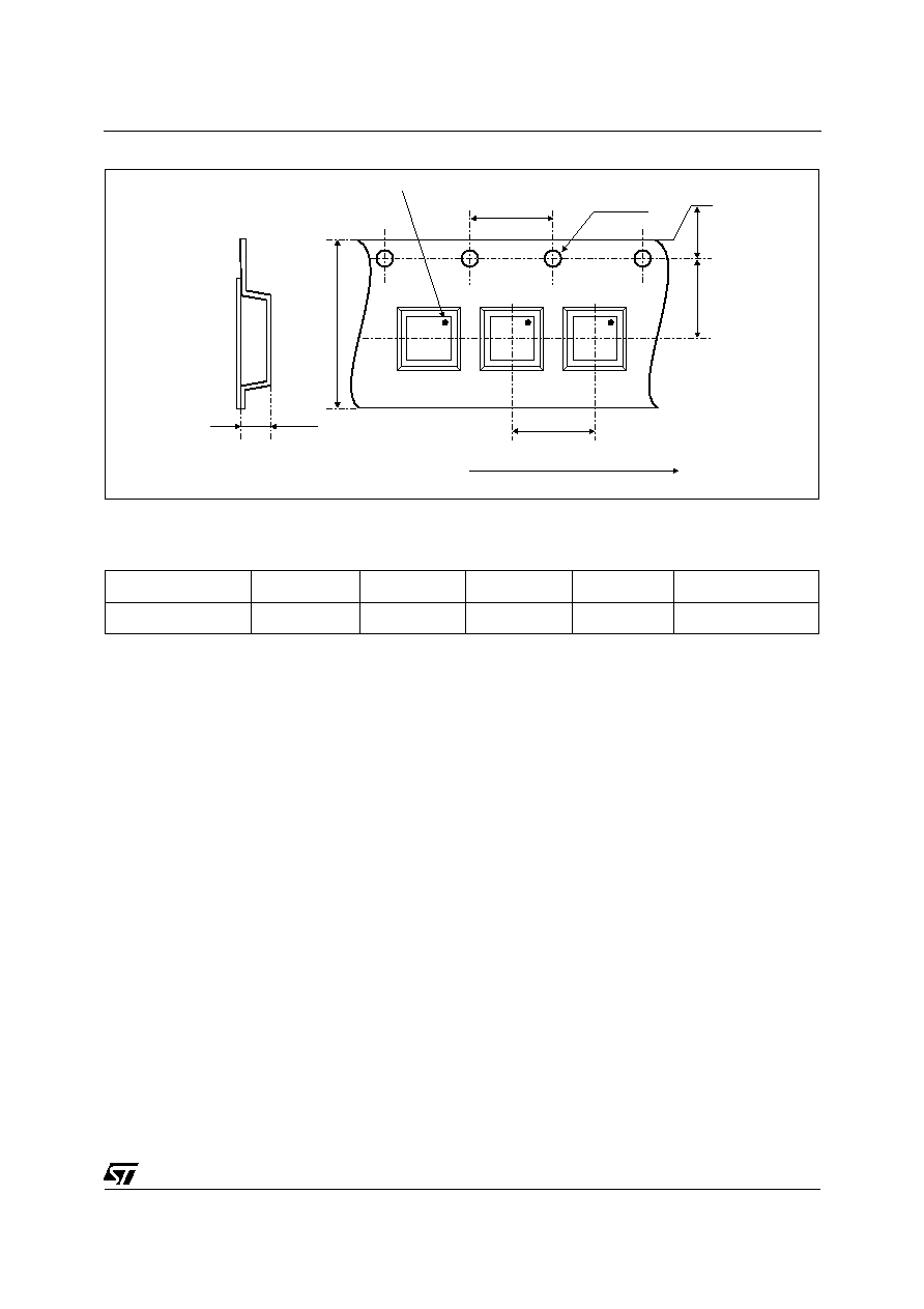
1.57mm ± 50µm
1.57mm ± 50µm
315µm ± 50
500µm ± 50
500µm ± 50
650µm ± 65
PACKAGE MECHANICAL DATA
365
365
240
40
220
x
y
x
w
x
w
Dot, ST logo
xxx = marking
yww = datecode
(y = year
ww = week)
All dimensions in µm
E
MARKING
Copper pad Diameter :
250µm recommended , 300µm max
Solder stencil opening : 330µm
Solder mask opening recommendation :
340µm min for 300µm copper pad diameter
FOOT PRINT RECOMMENDATIONS
STPAC02F1
5/5
Information furnished is believed to be accurate and reliable. However, STMicroelectronics assumes no responsibility for the consequences of
use of such information nor for any infringement of patents or other rights of third parties which may result from its use. No license is granted by
implication or otherwise under any patent or patent rights of STMicroelectronics. Specifications mentioned in this publication are subject to
change without notice. This publication supersedes and replaces all information previously supplied. STMicroelectronics products are not au-
thorized for use as critical components in life support devices or systems without express written approval of STMicroelectronics.
The ST logo is a registered trademark of STMicroelectronics.
All other names are the property of their respective owners.
© 2003 STMicroelectronics - All rights reserved.
STMicroelectronics GROUP OF COMPANIES
Australia - Belgium - Brazil - Canada - China - Czech Republic - Finland - France - Germany -
Hong Kong - India - Israel - Italy - Japan - Malaysia - Malta - Morocco - Singapore - Spain -
Sweden - Switzerland - United Kingdom - United States
www.st.com
Note: More packing informations are available in the application notes:
AN1235: ''Flip-Chip: Package description and recommandations for use''
AN1751: "EMI Filters: Recommendations and measurements"
Dot identifying Pin A1 location
User direction of unreeling
All dimensions in mm
4 +/- 0.1
8 +/- 0.3
4 +/- 0.1
1.75 +/- 0.1
3
.5 +/- 0.1
ÿ 1.5 +/- 0.1
0.73 +/- 0.05
xxx
yww
ST
E
xxx
yww
ST
E
xxx
yww
ST
E
FLIP-CHIP TAPE AND REEL SPECIFICATION
Ordering code
Marking
Package
Weight
Base qty
Delivery mode
STPAC02F1
RBT
Flip-Chip
3.3 mg
5000
Tape & reel
OTHER INFORMATION