ULTRA-FAST RECOVERY RECTIFIER DIODES
1/7
STPR1620CG/CT/CR
®
Octobert 2002 - Ed: 3C
ULTRA-FAST RECOVERY RECTIFIER DIODES
D
2
PAK
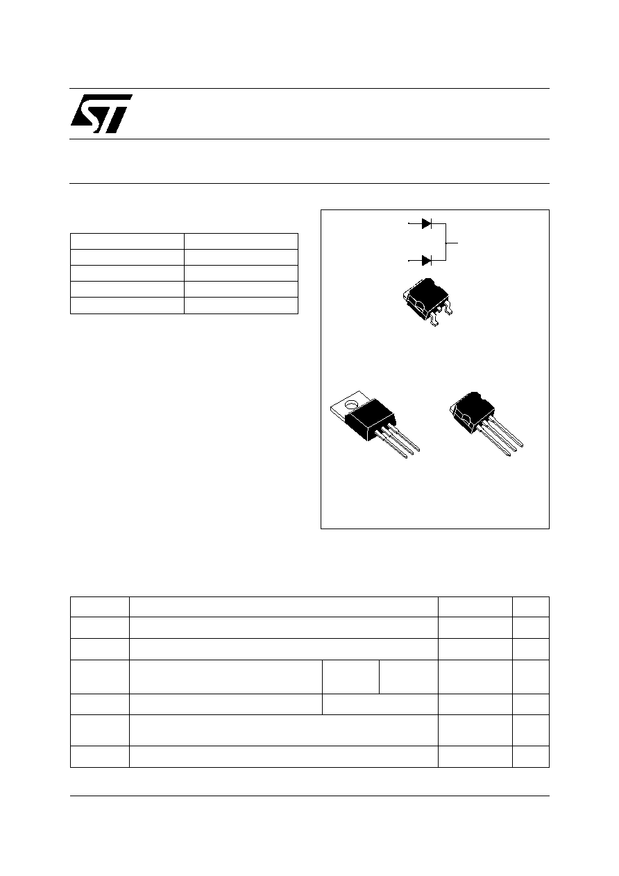
STPR1620CG
s
SUITED FOR SMPS
s
LOW LOSSES
s
LOW FORWARD AND REVERSE RECOVERY
TIME
s
HIGH SURGE CURRENT CAPABILITY
FEATURES
Low cost dual center tap rectifier suited for
Switched
Mode
Power
Supplies
and
high
frequency DC to DC converters.
Packaged in D
2
PAK, I
2
PAK or TO-220AB, this
device is intended for use in low voltage, high
frequency inverters, free wheeling and polarity
protection applications.
DESCRIPTION
Symbol
Parameter
Value
Unit
V
RRM
Repetitive peak reverse voltage
200
V
I
F(RMS)
RMS forward current
20
A
I
F(AV)
Average forward current
= 0.5
Tc=120°C
Per diode
Per device
8
16
A
I
FSM
Surge non repetitive forward current
tp=10ms sinusoidal
80
A
T
stg
Storage temperature range
- 65 to +
150
°C
Tj
Maximum operating junction temperature
150
°
C
ABSOLUTE RATINGS (limiting values, per diode)
K
K
A2
A1
A1
K
A2
I
F(AV)
2 x 8 A
V
RRM
200 V
Tj (max)
150°C
V
F
(max)
0.99 V
trr (max)
30 ns
MAIN PRODUCTS CHARACTERISTICS
TO-220AB
STPR1620CT
A1
A2
K
A1
K
A2
I
2
PAK
STPR1620CR
STPR1620CG / STPR1620CT / STPR1620CR
2/7
Symbol
Test conditions
Min.
Typ.
Max.
Unit
I
R
*
T
j
= 25°C
V
R
= V
RRM
50
µ
A
T
j
= 100°C
0.2
0.6
mA
V
F **
T
j
= 125
°
C
I
F
= 8 A
0.8
0.99
V
T
j
= 125
°
C
I
F
= 16 A
0.95
1.20
T
j
= 25
°
C
I
F
= 16 A
1.25
Pulse test : * tp = 5 ms,
< 2 %
** tp = 380
µ
s,
< 2 %
To evaluate the conduction losses use the following equation :
P = 0.78 x I
F(AV)
+ 0.026 x I
F
2
(RMS)
STATIC ELECTRICAL CHARACTERISTICS
Symbol
Test conditions
Min.
Typ.
Max.
Unit
trr
T
j
= 25°C
I
F
= 0.5A
I
R
= 1A
Irr = 0.25A
30
ns
tfr
T
j
= 25
°
C
I
F
= 3A
V
FR
= 1.1 x V
F
max
dI
F
/dt = 50 A/
µ
s
20
ns
V
FP
T
j
= 25
°
C
I
F
= 3A
dI
F
/dt = 50 A/
µ
s
3
V
RECOVERY CHARACTERISTICS
Symbol
Parameter
Value
Unit
R
th (j-c)
Junction to case
Per diode
3.0
°
C/W
Total
1.8
°
C/W
R
th (c)
Coupling
0.6
°
C/W
When the diodes 1 and 2 are used simultaneously :
Tj(diode 1) = P(diode 1) x Rth(j-c) (Per diode) + P(diode 2) x Rth(c)
THERMAL RESISTANCES
STPR1620CG / STRP1620CT / STPR1620CR
3/7
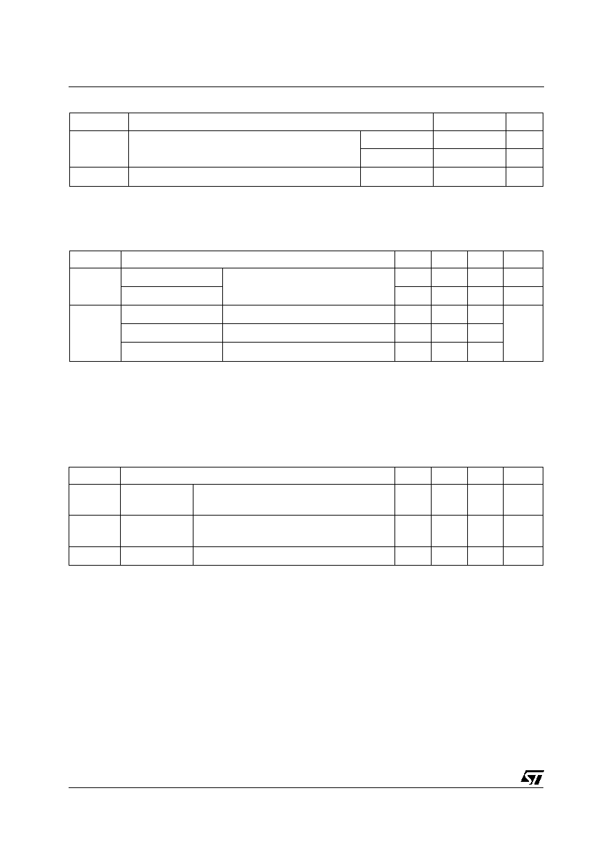
Fig. 2: Peak current versus form factor (per diode).
Fig. 3: Average
current
versus
ambient
temperature (
: 0.5, per diode).
Fig. 4: Non repetitive surge peak forward current
versus overload duration (maximum values, per
diode).
Fig. 1: Average forward power dissipation versus
average forward current (per diode).
Fig. 5: Relative variation of thermal transient
impedance junction to case versus pulse duration
(per diode).
Fig. 6: Forward voltage drop versus forward
current (maximum values, per diode).
STPR1620CG / STPR1620CT / STPR1620CR
4/7
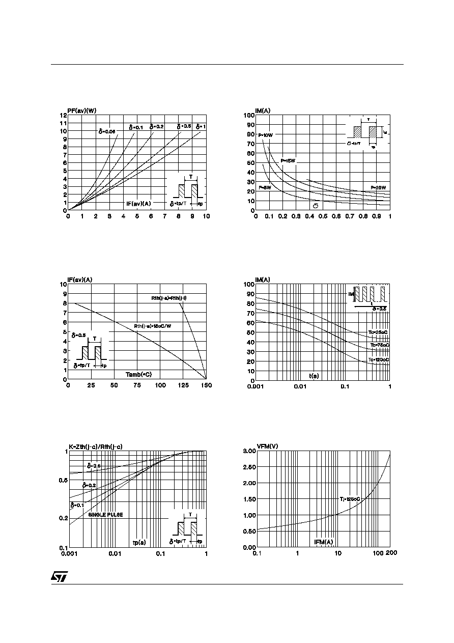
H
Fig. 7: Junction capacitance versus reverse
voltage applied (typical values, per diode).
Fig. 8: Recovery charges versus dI
F
/dt (per
diode).
Fig. 10: Dynamic parameters versus junction
temperature (per diode).
Fig. 9: Peak reverse current versus dI
F
/dt (per
diode).
0
2
4
6
8
10
12
14
16
18
20
0
10
20
30
40
50
60
70
80
S(Cu) (cm²)
Rth(j-a) (°C/W)
Fig. 11: Thermal resistance junction to ambient
versus copper surface under tab (epoxy printed
circuit board, CU = 35µs) (STPR1620CG only).
STPR1620CG / STRP1620CT / STPR1620CR
5/7
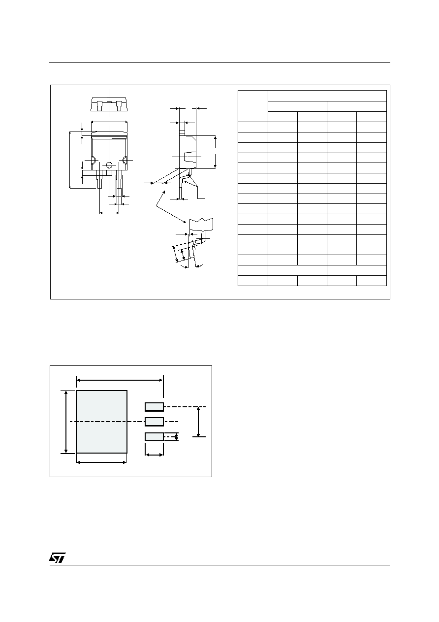
PACKAGE MECHANICAL DATA
D
2
PAK (Plastic)
A
C2
D
R
A2
M
V2
C
A1
G
L
L3
L2
B
B2
E
*
* FLAT ZONE NO LESS THAN 2mm
REF.
DIMENSIONS
Millimeters
Inches
Min.
Max.
Min.
Max.
A
4.40
4.60
0.173
0.181
A1
2.49
2.69
0.098
0.106
A2
0.03
0.23
0.001
0.009
B
0.70
0.93
0.027
0.037
B2
1.14
1.70
0.045
0.067
C
0.45
0.60
0.017
0.024
C2
1.23
1.36
0.048
0.054
D
8.95
9.35
0.352
0.368
E
10.00
10.40
0.393
0.409
G
4.88
5.28
0.192
0.208
L
15.00
15.85
0.590
0.624
L2
1.27
1.40
0.050
0.055
L3
1.40
1.75
0.055
0.069
M
2.40
3.20
0.094
0.126
R
0.40 typ.
0.016 typ.
V2
0°
8°
0°
8°
8.90
3.70
1.30
5.08
16.90
10.30
FOOT PRINT (in millimeters)