Rev 1
November 2005
1/7
7
STPS200170TV1
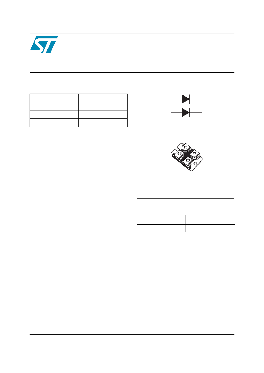
High voltage power Schottky rectifier
Main product characteristics
Features and benefits
Negligible switching losses
Avalanche rated
Low leakage current
Good trade-off between leakage current and
forward voltage drop
Insulated package
≠ ISOTOP
Electrical insulation = 2500 V
RMS
Capacitance = 45 pF
Description
High voltage Schottky rectifier suited for high
frequency switch mode power supply.
Packaged in ISOTOP, this device is intended for
use in the secondary rectification of the
applications.
Order codes
I
F(AV)
2 x 100 A
V
RRM
170 V
T
j
150 ∞C
V
F
(typ)
0.63 V
Part Number
Marking
STPS200170TV1
STPS200170TV1
A1
K1
A2
K2
A1
K1
A2
K2
ISOTOP
www.st.com
1 Characteristics
STPS200170TV1
2/7
1 Characteristics
When the diodes are used simultaneously:
T
j(diode1)
= P
(diode1)
X
R
th(j-c)
(per diode) + P
(diode2)
X
R
th(c)
To evaluate the conduction losses use the following equation: P = 0.5 x I
F(AV)
+ 0.0018 I
F
2
(RMS)
Table 1.
Absolute ratings - limiting values per diode at T
amb
= 25 ∞C, unless otherwise specified
Symbol
Parameter
Value
Unit
V
RRM
Repetitive peak reverse voltage
170
V
I
F(RMS)
RMS forward current
200
A
I
F(AV)
Average forward current,
= 0.5
T
c
= 105 ∞C per diode
100
A
I
FSM
Surge non repetitive forward current t
p
= 10 ms Sinusoidal
700
A
P
ARM
Repetitive peak avalanche power
t
p
= 1 µs, T
j
= 25 ∞C
100000
W
T
stg
Storage temperature range
-55 to + 150
∞C
T
j
Maximum operating junction temperature
(1)
1.
thermal runaway condition for a diode on its own heatsink
150
∞C
Table 2.
Thermal parameters
Symbol
Parameter
Value
Unit
R
th(j-c)
Junction to case
Per diode
0.52
∞C/W
Total
0.31
R
th(c)
Coupling thermal resistance
0.1
Table 3.
Static electrical characteristics
Symbol
Parameter
Test conditions
Min.
Typ
Max.
Unit
I
R
(1)
1.
Pulse test: t
p
= 5 ms,
< 2 %
Reverse leakage current
T
j
= 25 ∞C
V
R
= V
RRM
200
µA
T
j
= 125 ∞C
30
100
mA
V
F
(2)
2.
Pulse test: t
p
= 380 µs,
< 2 %
Forward voltage drop
T
j
= 25 ∞C
I
F
= 100 A
0.83
V
T
j
= 150 ∞C
0.63
0.68
T
j
= 25 ∞C
I
F
= 200 A
0.975
T
j
= 150 ∞C
0.78
0.86
dP
tot
dT
j
---------------
1
R
th j
a
≠
(
)
--------------------------
<
STPS200170TV1
1 Characteristics
3/7
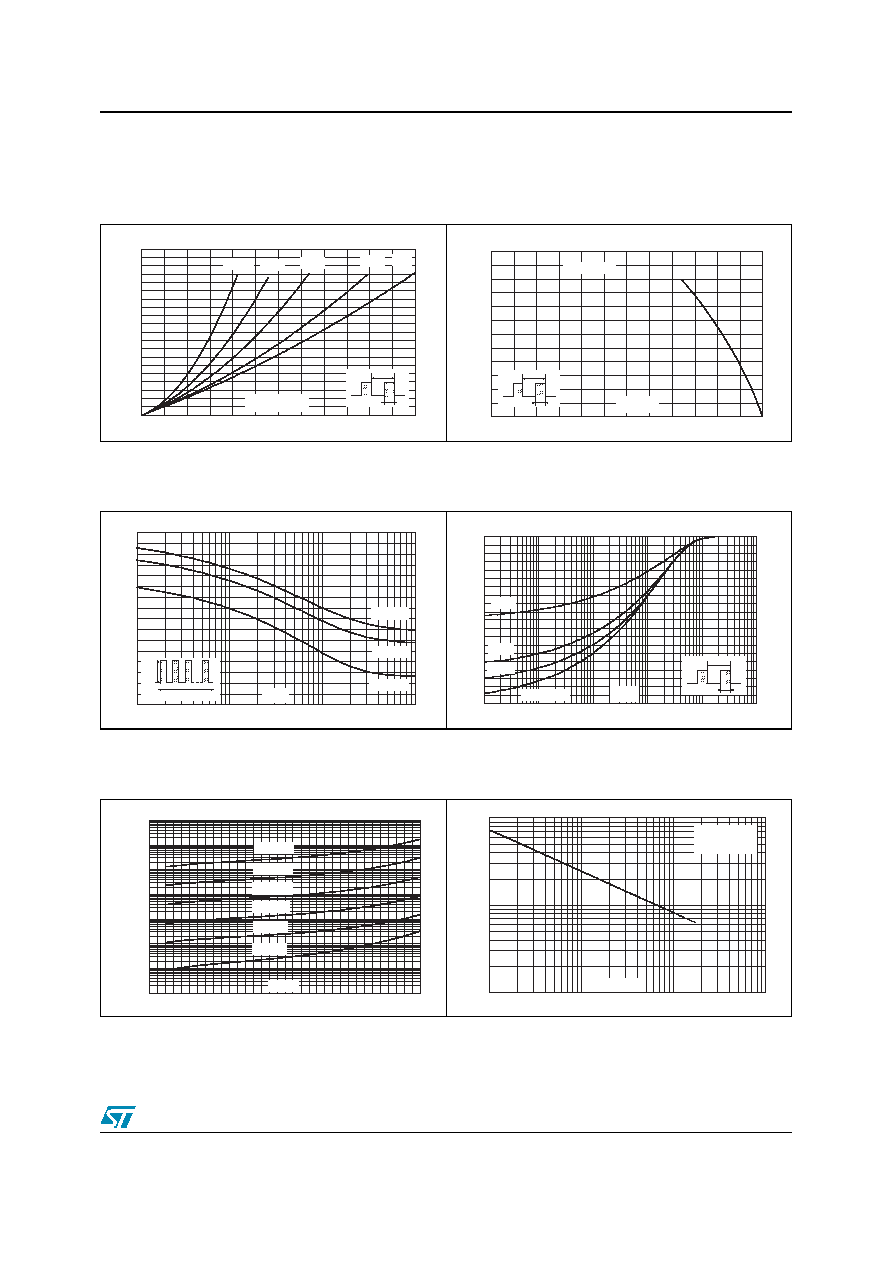
Figure 1.
Conduction losses versus average
current (per diode)
Figure 2.
Average forward current versus
ambient temperature
(
= 0.5, per diode)
Figure 3.
Non-repetitive surge peak forward
current vesus overload duration
(maximum values per diode)
Figure 4.
Relative variation of thermal
impedance (junction to case) versus
pulse duration
Figure 5.
Reverse leakage current versus
reverse voltage applied (typical
values per diode)
Figure 6.
Junction capacitances versus
reverse voltage applied (typical
values per diode)
0
10
20
30
40
50
60
70
80
90
100
0
20
40
60
80
100
120
P
F(AV)
(W)
=0.05
=0.1
=0.2
=0.5
=1
T
=t /T
p
tp
I
F(AV)
(A)
0
20
40
60
80
100
120
0
25
50
75
100
125
150
I
F(AV)
(A)
T
=tp/T
tp
R
th(j-a)
=R
th(j-c)
T
amb
(∞C)
0
100
200
300
400
500
600
700
800
1.E-03
1.E-02
1.E-01
1.E+00
I
M
(A)
T
C
=50∞C
T
C
=75∞C
T
C
=125∞C
I
M
t
d
=0.5
t(s)
0.0
0.1
0.2
0.3
0.4
0.5
0.6
0.7
0.8
0.9
1.0
1.E-04
1.E-03
1.E-02
1.E-01
1.E+00
1.E+01
(j )
(j )
=0.1
=0.2
=0.5
Single pulse
T
=tp/T
tp
Z
th -c
/R
th -c
t
P
(s)
1.E-04
1.E-03
1.E-02
1.E-01
1.E+00
1.E+01
1.E+02
1.E+03
0
10 20 30 40 50 60 70 80 90 100 110 120 130 140 150 160 170
I
R
(mA)
T
j
=150∞C
T
j
=125∞C
T
j
=25∞C
T
j
=100∞C
T
j
=75∞C
T
j
=50∞C
V
R
(V)
100
1000
10000
1
10
100
1000
C(pF)
F=1MHz
V
OSC
=30mV
RMS
T
j
=25∞C
V
R
(V)
1 Characteristics
STPS200170TV1
4/7
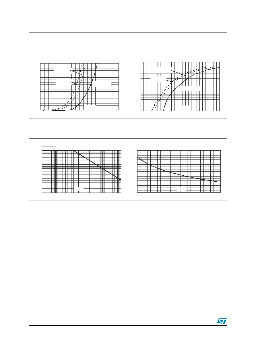
Figure 7.
Forward voltage drop versus
forward current
(per diode, low level)
Figure 8.
Forward voltage drop versus
forward current
(per diode, high level)
Figure 9.
Normalized avalanche power
derating versus pulse duration
Figure 10. Normalized avalanche power
derating versus junction
temperature
0
5
10
15
20
25
30
35
40
45
50
0.0
0.1
0.2
0.3
0.4
0.5
0.6
0.7
0.8
0.9
1.0
I
FM
(A)
Tj=25∞C
(Maximum values)
Tj=150∞C
(Maximum values)
Tj=150∞C
(Maximum values)
Tj=150∞C
(Typical values)
Tj=150∞C
(Typical values)
V
FM
(V)
1
10
100
1000
0.0
0.1
0.2
0.3
0.4
0.5
0.6
0.7
0.8
0.9
1.0
1.1
1.2
1.3
1.4
I
FM
(A)
Tj=25∞C
(Maximum values)
Tj=150∞C
(Maximum values)
Tj=150∞C
(Maximum values)
Tj=150∞C
(Typical values)
Tj=150∞C
(Typical values)
V
FM
(V)
0.001
0.01
0.1
0.01
1
0.1
10
100
1000
1
t (µs)
p
P
(t )
P
(1µs)
ARM p
ARM
0
0.2
0.4
0.6
0.8
1
1.2
25
50
75
100
125
150
T (∞C)
j
P
(t )
P
(25∞C)
ARM p
ARM
STPS200170TV1
2 Package mechanical data
5/7
2 Package
mechanical
data
Epoxy meets UL94, V0
Cooling method: by conduction (C)
In order to meet environmental requirements, ST offers these devices in ECOPACKÆ
packages. These packages have a Lead-free second level interconnect . The category of
second level interconnect is marked on the package and on the inner box label, in compliance
with JEDEC Standard JESD97. The maximum ratings related to soldering conditions are also
marked on the inner box label. ECOPACK is an ST trademark. ECOPACK specifications are
available at: www.st.com.
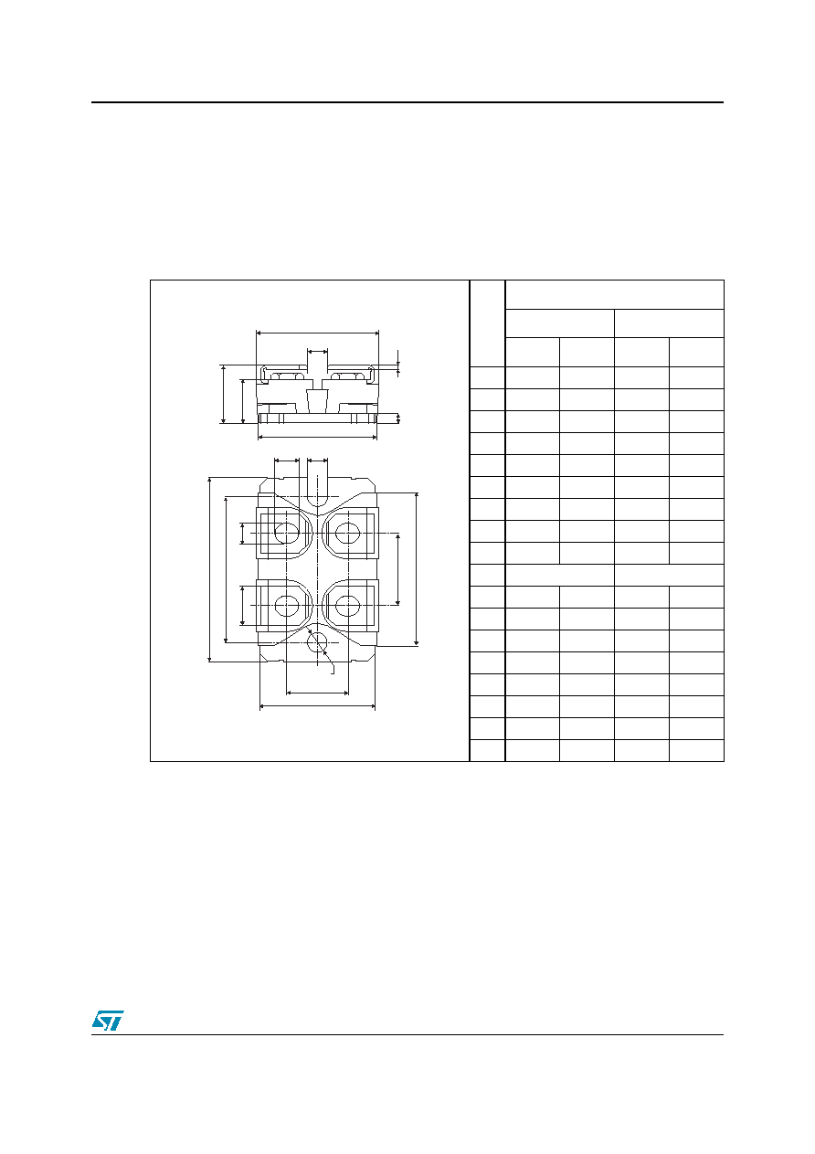
Table 4.
ISOTOP dimensions
REF.
DIMENSIONS
Millimeters
Inches
Min.
Max
Min.
Max.
A
11.80
12.20
0.465
0.480
A1
8.90
9.10
0.350
0.358
B
7.8
8.20
0.307
0.323
C
0.75
0.85
0.030
0.033
C2
1.95
2.05
0.077
0.081
D
37.80
38.20
1.488
1.504
D1
31.50
31.70
1.240
1.248
E
25.15
25.50
0.990
1.004
E1
23.85
24.15
0.939
0.951
E2
24.80 typ.
0.976 typ.
G
14.90
15.10
0.587
0.594
G1
12.60
12.80
0.496
0.504
G2
3.50
4.30
0.138
0.169
F
4.10
4.30
0.161
0.169
F1
4.60
5.00
0.181
0.197
P
4.00
4.30
0.157
0.69
P1
4.00
4.40
0.157
0.173
S
30.10
30.30
1.185
1.193
F1
F
D1
G
D
S
B
E1
G1
ÿP
P1
E
E2
G2
C
C2
A1
A