1/5
STPS20170CT
Æ
March 2004 - Ed: 1
HIGH VOLTAGE POWER SCHOTTKY RECTIFIER
I
F(AV)
2 x 10 A
V
RRM
170 V
T
j
175∞C
V
F
(max)
0.75 V
MAIN PRODUCT CHARACTERISTICS
HIGH JUNCTION TEMPERATURE CAPABILITY
GOOD TRADE OFF BETWEEN LEAKAGE
CURRENT AND FORWARD VOLTAGE DROP
LOW LEAKAGE CURRENT
AVALANCHE CAPABILITY SPECIFIED
FEATURES AND BENEFITS
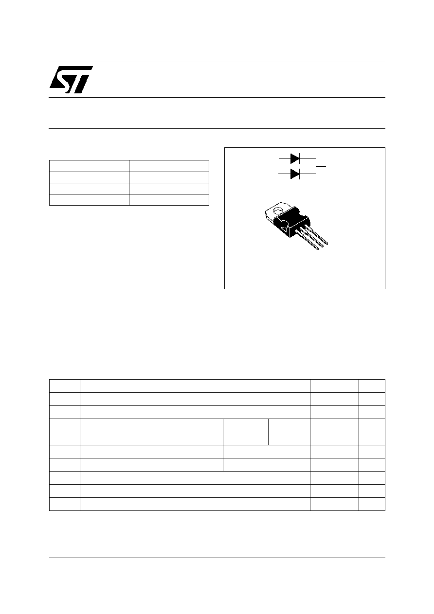
Dual center tap schottky rectifier designed for
high
frequency
Switched
Mode
Power
Supplies.
DESCRIPTION
Symbol
Parameter
Value
Unit
V
RRM
Repetitive peak reverse voltage
170
V
I
F(RMS)
RMS forward current
30
A
I
F(AV)
Average forward current
= 0.5
Tc = 155∞C
Per diode
10
A
Per device
20
I
FSM
Surge non repetitive forward current
tp = 10 ms sinusoidal
180
A
P
ARM
Repetitive peak avalanche power
tp = 1µs
Tj = 25∞C
6700
W
T
stg
Storage temperature range
- 65 to + 175
∞C
T
j
Maximum operating junction temperature*
175
∞C
dV/dt
Critical rate of rise of reverse voltage
10000
V/µs
* Thermal runaway condition for a diode on its own heatsink
Ptot/Tj < 1/(Rth(j-a))
ABSOLUTE RATINGS (limiting values, per diode)
A1
A2
K
TO-220AB
STPS20150CT
A1
A2
K
STPS20170CT
2/5
Symbol
Parameter
Value
Unit
R
th(j-c)
Junction to case
Per diode
2.2
∞C/W
Total
1.3
R
th(c)
Coupling
0.3
THERMAL RESISTANCES
Symbol
Parameter
Tests conditions
Min.
Typ.
Max.
Unit
I
R
*
Reverse leakage current
Tj = 25∞C
V
R
= V
RRM
15
µA
Tj = 125∞C
15
mA
V
F
**
Forward voltage drop
Tj = 25
∞C
I
F
= 10 A
0.90
V
Tj = 125∞C
I
F
= 10 A
0.69
0.75
Tj = 25
∞C
I
F
= 20 A
0.99
Tj = 125∞C
I
F
= 20 A
0.79
0.86
Pulse test :
* tp = 5 ms,
< 2%
** tp = 380 µs,
< 2%
To evaluate the conduction losses use the following equation:
P = 0.64 x I
F(AV)
+ 0.011 I
F
2
(RMS)
STATIC ELECTRICAL CHARACTERISTICS (per diode)
When the diodes 1 and 2 are used simultaneously :
Tj(diode 1) = P(diode1) x R
th(j-c)
(Per diode) + P(diode 2) x R
th(c)
STPS20170CT
3/5
P
(W)
F(AV)
0
1
2
3
4
5
6
7
8
9
10
0
1
2
3
4
5
6
7
8
9
10
11
12
I
(A)
F(AV)
T
=tp/T
tp
= 0.05
= 0.1
= 0.2
= 0.5
= 1
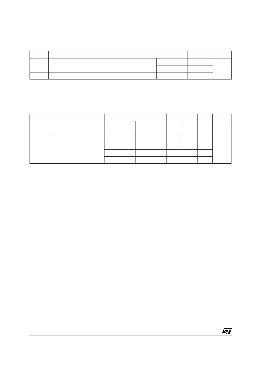
Fig. 1: Average forward power dissipation versus
average forward current (per diode).
I
(A)
F(AV)
0
1
2
3
4
5
6
7
8
9
10
11
12
0
25
50
75
100
125
150
175
T
(∞C)
amb
T
=tp/T
tp
R
=15∞C/W
th(j-a)
R
=R
th(j-a)
th(j-c)
Fig. 2: Average forward current versus ambient
temperature (
= 0.5, per diode).
0
0.2
0.4
0.6
0.8
1
1.2
0
25
50
75
100
125
150
T (∞C)
j
P
(t )
P
(25∞C)
ARM p
ARM
Fig. 4: Normalized avalanche power derating
versus junction temperature.
0.001
0.01
0.1
0.01
1
0.1
10
100
1000
1
t (µs)
p
P
(t )
P
(1µs)
ARM p
ARM
Fig. 3: Normalized avalanche power derating ver-
sus pulse duration.
0
25
50
75
100
125
150
1.E-03
1.E-02
1.E-01
1.E+00
t(s)
I (A)
M
I
M
t
=0.5
T =50∞C
C
T =75∞C
C
T =125∞C
C
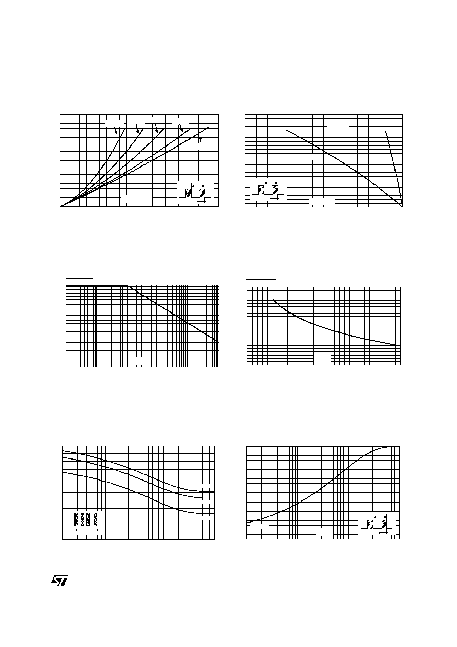
Fig. 5: Non repetitive surge peak forward current
versus overload duration (maximum values, per
diode).
0.0
0.1
0.2
0.3
0.4
0.5
0.6
0.7
0.8
0.9
1.0
1.E-03
1.E-02
1.E-01
1.E+00
t (s)
p
Z
/R
th(j-c)
th(j-c)
T
=tp/T
tp
Single pulse
Fig. 6: Relative variation of thermal impedance
junction to case versus pulse duration.
STPS20170CT
4/5
1.E-01
1.E+00
1.E+01
1.E+02
1.E+03
1.E+04
1.E+05
0
25
50
75
100
125
150
175
I (µA)
R
V (V)
R
T =175∞C
j
T =150∞C
j
T =125∞C
j
T =100∞C
j
T =25∞C
j
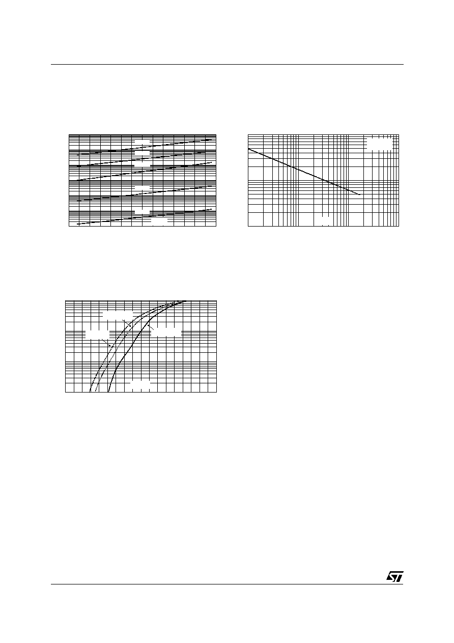
Fig. 7: Reverse leakage current versus reverse
voltage applied (typical values, per diode).
10
100
1000
1
10
100
1000
C(pF)
V (V)
R
F=1MHz
V
=30mV
T =25∞C
OSC
RMS
j
Fig. 8: Junction capacitance versus reverse voltage
applied (typical values, per diode).
I
(A)
FM
0.1
1.0
10.0
100.0
0.0
0.2
0.4
0.6
0.8
1.0
1.2
1.4
1.6
1.8
T =125∞C
(typical values)
j
T =125∞C
(maximum values)
j
T =25∞C
(maximum values)
j
V
(V)
FM
Fig. 9: Forward voltage drop versus forward
current (per diode).
STPS20170CT
5/5
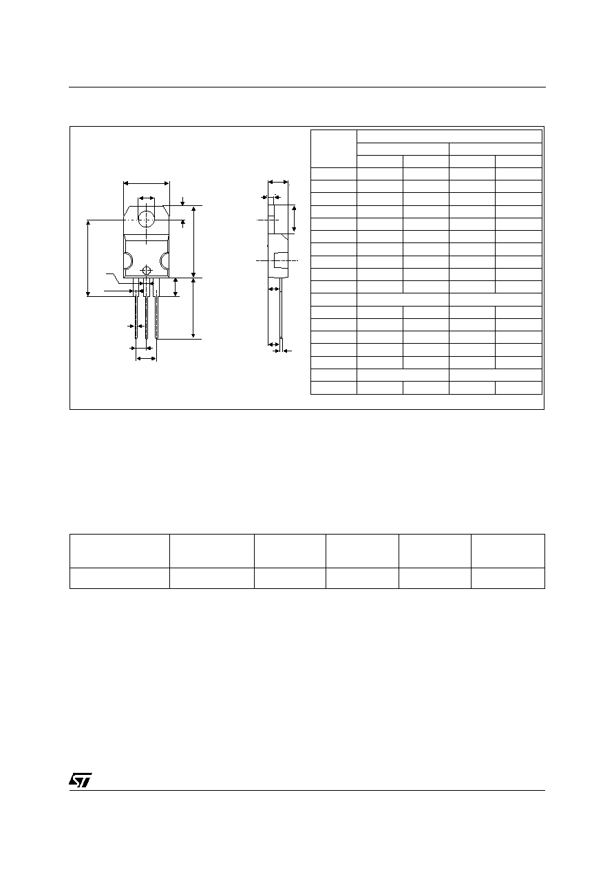
PACKAGE MECHANICAL DATA
TO-220AB
A
C
D
L7
Dia
L5
L6
L9
L4
F
H2
G
G1
L2
F2
F1
E
M
REF.
DIMENSIONS
Millimeters
Inches
Min.
Max.
Min.
Max.
A
4.40
4.60
0.173
0.181
C
1.23
1.32
0.048
0.051
D
2.40
2.72
0.094
0.107
E
0.49
0.70
0.019
0.027
F
0.61
0.88
0.024
0.034
F1
1.14
1.70
0.044
0.066
F2
1.14
1.70
0.044
0.066
G
4.95
5.15
0.194
0.202
G1
2.40
2.70
0.094
0.106
H2
10
10.40
0.393
0.409
L2
16.4 typ.
0.645 typ.
L4
13
14
0.511
0.551
L5
2.65
2.95
0.104
0.116
L6
15.25
15.75
0.600
0.620
L7
6.20
6.60
0.244
0.259
L9
3.50
3.93
0.137
0.154
M
2.6 typ.
0.102 typ.
Diam.
3.75
3.85
0.147
0.151
Information furnished is believed to be accurate and reliable. However, STMicroelectronics assumes no responsibility for the consequences of
use of such information nor for any infringement of patents or other rights of third parties which may result from its use. No license is granted by
implication or otherwise under any patent or patent rights of STMicroelectronics. Specifications mentioned in this publication are subject to
change without notice. This publication supersedes and replaces all information previously supplied. STMicroelectronics products are not au-
thorized for use as critical components in life support devices or systems without express written approval of STMicroelectronics.
The ST logo is a registered trademark of STMicroelectronics.
All other names are the property of their respective owners.
© 2004 STMicroelectronics - All rights reserved.
STMicroelectronics GROUP OF COMPANIES
Australia - Belgium - Brazil - Canada - China - Czech Republic - Finland - France - Germany -
Hong Kong - India - Israel - Italy - Japan - Malaysia - Malta - Morocco - Singapore - Spain -
Sweden - Switzerland - United Kingdom - United States
www.st.com
Ordering type
Marking
Package
Weight
Base qty
Delivery
mode
STPS20170CT
STPS20170CT
TO-220AB
2.20 g
50
Tube
EPOXY MEETS UL94,V0
OTHER INFORMATION