July 2006
Rev 1
1/7
7
STPS2060C
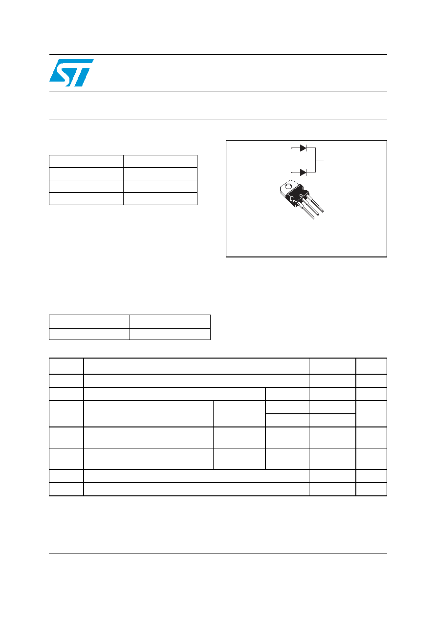
High voltage power Schottky rectifier
Main product characteristics
Description
High voltage dual Schottky rectifier suited for
switch mode power supplies and other power
converters.
Packaged in TO-220, this device is intended for
use in medium voltage operation, and particularly,
in high frequency circuitries where low switching
losses and low noise are required.
Order code
Features and benefits
Negligible switching losses
Low forward voltage drop
Low capacitance
High reverse avalanche surge capability
Avalanche rated
I
F(AV)
2 x 10 A
V
RRM
60 V
T
j
(max)
150� C
V
F
(max)
0.7 V
Part Number
Marking
STPS2060CT
STPS2060CT
A1
K
A2
A1
A2
K
TO-220AB
STPS2060CT
Table 1.
Absolute ratings (limiting values, per diode at 25� C, unless otherwise specified)
Symbol
Parameter
Value
Unit
V
RRM
Repetitive peak reverse voltage
60
V
I
F(RMS)
RMS forward current
Per diode
20
A
I
F(AV)
Average forward current
= 0.5
T
c
= 135� C
Per diode
10
A
Per device
20
I
FSM
Surge non repetitive forward current
t
p
= 10 ms
sinusoidal
Per diode
200
A
P
ARM
Repetitive peak avalanche power
t
p
= 1 �s
T
j
= 25� C
Per device
10800
W
T
stg
Storage temperature range
-65 to + 150
�C
T
j
Maximum operating junction temperature
(1)
1.
condition to avoid thermal runaway for a diode on its own heatsink
150
�C
dPtot
dTj
---------------
1
Rth j
a
�
(
)
--------------------------
<
www.st.com
Characteristics
STPS2060C
2/7
1 Characteristics
When the diodes 1 and 2 are used simultaneously:
T
j
(diode 1) = P(diode1) x R
th(j-c)
(Per diode) + P(diode 2) x R
th(c)
Table 2.
Thermal resistance
Symbol
Parameter
Value
Unit
R
th(j-c)
Junction to case
Per diode
1.6
�C/W
Total
0.9
R
th(c)
Coupling
0.15
Table 3.
Static electrical characteristics (per diode)
Symbol
Parameter
Test conditions
Min.
Typ.
Max.
Unit
I
R
(1)
Reverse leakage current
T
j
= 25� C
V
R
= V
RRM
150
�A
T
j
= 125� C
100
mA
V
F
(2)
Forward voltage drop
T
j
= 25� C
I
F
= 10 A
0.80
V
T
j
= 125� C
I
F
= 10 A
0.60
0.70
T
j
= 25� C
I
F
= 20 A
0.94
T
j
= 125� C
I
F
= 20 A
0.75
0.85
1.
Pulse test: tp = 5 ms,
< 2%
2.
Pulse test: tp = 380 �s,
< 2%
To evaluate the conduction losses use the following equation:
P = 0.55 x I
F(AV)
+ 0.015 I
F
2
(RMS)
STPS2060C
Characteristics
3/7
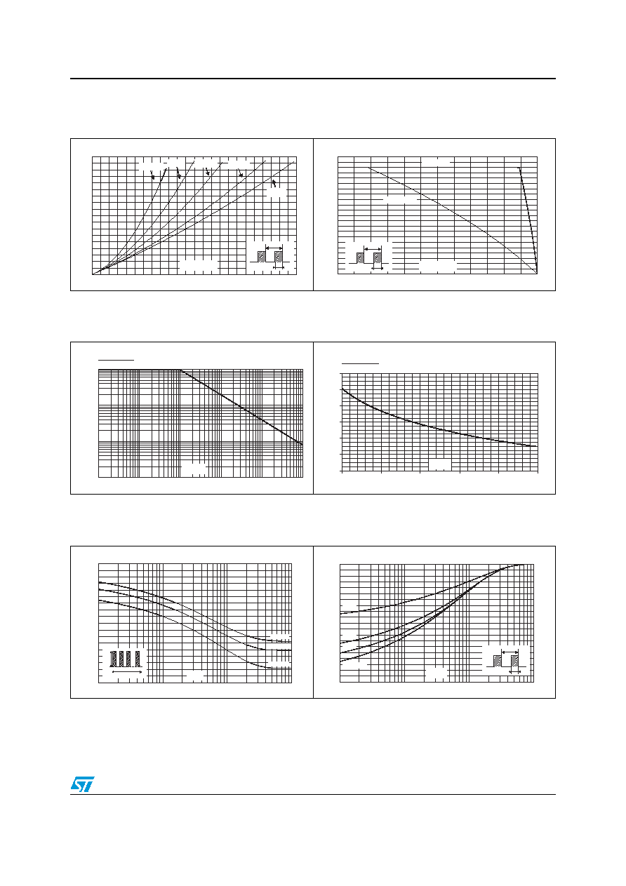
Figure 1.
Conduction losses versus average
current (per diode)
Figure 2.
Average forward current versus
ambient temperature (
= 0.5, per
diode)
0
1
2
3
4
5
6
7
8
9
0
1
2
3
4
5
6
7
8
9
10
11
12
P
(W)
F(AV)
I
(A)
F(AV)
T
=tp/T
tp
= 0.05
= 0.1
= 0.2
= 1
= 0.5
0
1
2
3
4
5
6
7
8
9
10
11
0
25
50
75
100
125
150
I
(A)
F(AV)
T
(�C)
amb
T
=tp/T
tp
R
=R
th(j-a)
th(j-c)
R
=15�C/W
th(j-a)
Figure 3.
Normalized avalanche power
derating versus pulse duration
Figure 4.
Normalized avalanche power
derating versus junction
temperature
0.001
0.01
0.1
0.01
1
0.1
10
100
1000
1
t (�s)
p
P
(t )
P
(1�s)
ARM p
ARM
0
0.2
0.4
0.6
0.8
1
1.2
25
50
75
100
125
150
T (�C)
j
P
(t )
P
(25�C)
ARM p
ARM
Figure 5.
Non repetitive surge peak forward
current versus overload duration
(maximum values, per diode)
Figure 6.
Relative variation of thermal
impedance junction to case versus
pulse duration
0
20
40
60
80
100
120
140
160
180
1.E-03
1.E-02
1.E-01
1.E+00
I (A)
M
I
M
t
=0.5
t(s)
T =50�C
C
T =75�C
C
T =110�C
C
0.0
0.1
0.2
0.3
0.4
0.5
0.6
0.7
0.8
0.9
1.0
1.E-03
1.E-02
1.E-01
1.E+00
Z
/R
th(j-c)
th(j-c)
T
=tp/T
tp
t (s)
p
= 0.5
= 0.2
= 0.1
Single pulse
Characteristics
STPS2060C
4/7
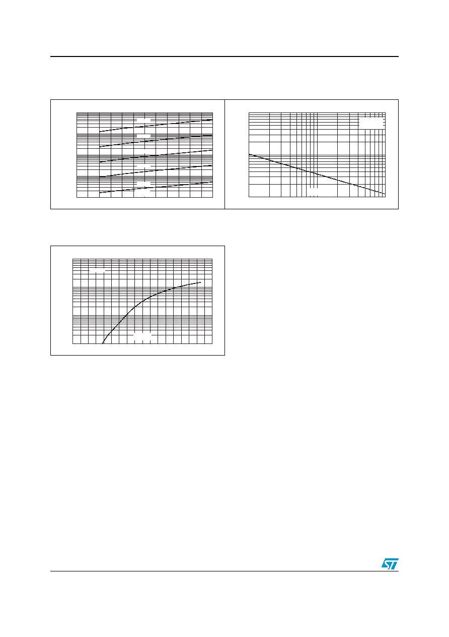
Figure 7.
Reverse leakage current versus
reverse voltage applied (typical
values, per diode)
Figure 8.
Junction capacitance versus
reverse voltage applied (typical
values, per diode)
Figure 9.
Forward voltage drop versus
forward current (maximum values,
per diode)
1.E-03
1.E-02
1.E-01
1.E+00
1.E+01
0
10
20
30
40
50
60
I (mA)
R
V (V)
R
T =125�C
j
T =100�C
j
T =50�C
j
T =25�C
j
T =75�C
j
100
1000
10000
1
10
100
C(pF)
V (V)
R
F=1MHz
V
=30mV
T =25�C
OSC
RMS
j
1
10
100
1000
0.0
0.2
0.4
0.6
0.8
1.0
1.2
1.4
1.6
1.8
I
(A)
FM
V
(V)
FM
T =125�C
j
STPS2060C
Package information
5/7
2 Package
information
Epoxy meets UL94,V0
Cooling Method: C
Recommended torque value: 0.55 Nm
Maximum torque value: 0.70 Nm
In order to meet environmental requirements, ST offers these devices in ECOPACK�
packages. These packages have a lead-free second level interconnect. The category of
second level interconnect is marked on the package and on the inner box label, in
compliance with JEDEC Standard JESD97. The maximum ratings related to soldering
conditions are also marked on the inner box label. ECOPACK is an ST trademark.
ECOPACK specifications are available at: www.st.com.
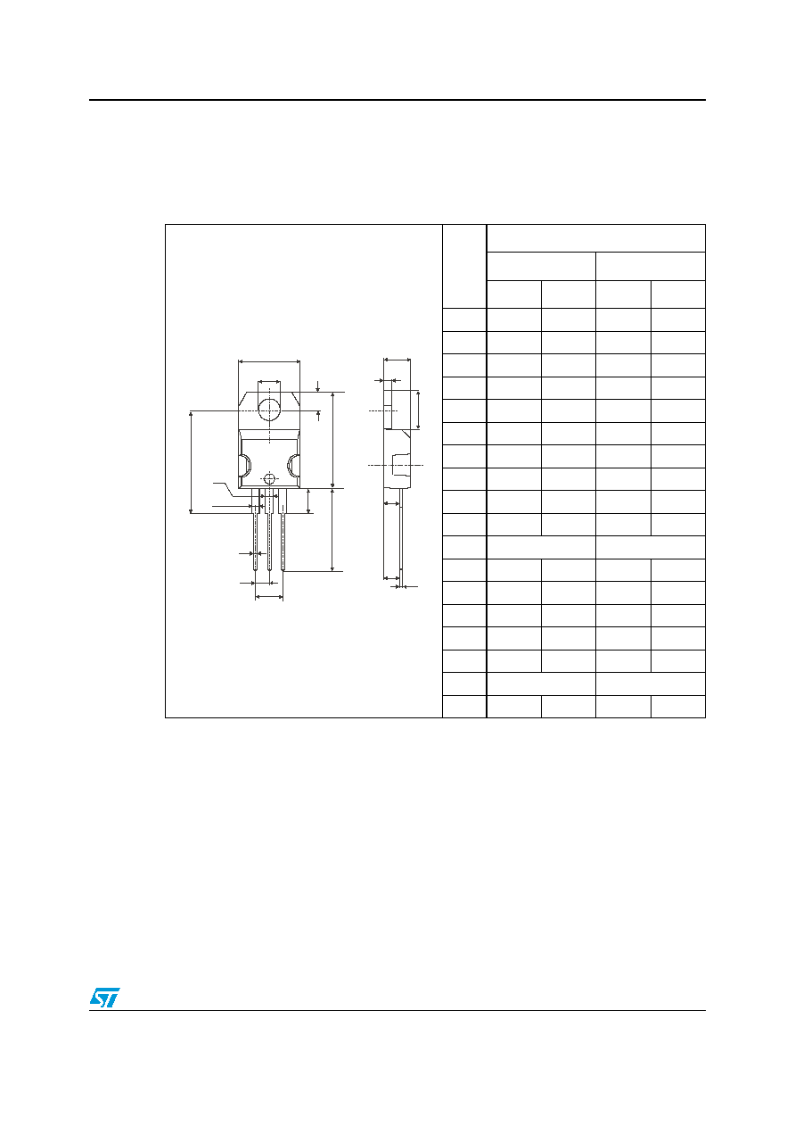
Table 4.
TO-220AB dimensions
Ref.
Dimensions
Millimeters
Inches
Min.
Max.
Min.
Max.
A
4.40
4.60
0.173
0.181
C
1.23
1.32
0.048
0.051
D
2.40
2.72
0.094
0.107
E
0.49
0.70
0.019
0.027
F
0.61
0.88
0.024
0.034
F1
1.14
1.70
0.044
0.066
F2
1.14
1.70
0.044
0.066
G
4.95
5.15
0.194
0.202
G1
2.40
2.70
0.094
0.106
H2
10
10.40
0.393
0.409
L2
16.4 typ.
0.645 typ.
L4
13
14
0.511
0.551
L5
2.65
2.95
0.104
0.116
L6
15.25
15.75
0.600
0.620
L7
6.20
6.60
0.244
0.259
L9
3.50
3.93
0.137
0.154
M
2.6 typ.
0.102 typ.
Diam.
3.75
3.85
0.147
0.151
A
C
D
L7
Dia
L5
L6
L9
L4
F
H2
G
G1
L2
F2
F1
E
M