Æ
1/7
Table 1: Main Product Characteristics
I
F(AV)
2 x 10 A
V
RRM
100 V
T
j
175∞C
V
F
(max)
0.71 V
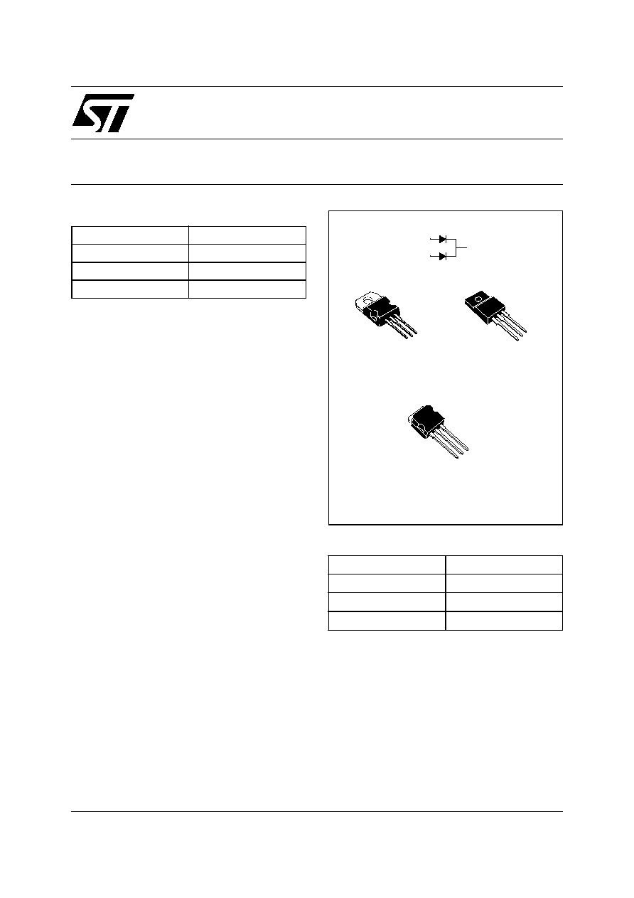
STPS20S100C
POWER SCHOTTKY RECTIFIER
REV. 1
K
A1
A2
K
A2
A1
K
K
A2
A1
K
A2
A1
TO-220AB
STPS20S100CT
TO-220FPAB
STPS20S100CFP
I
2
PAK
STPS20S100CR
March 2005
FEATURES AND BENEFITS
High junction temperature capability for
converters located in confined enrironment
Low leakage current at high temperature
Low static and dynamic losses as a result of the
Schottky barrier
Avalanche specification
DESCRIPTION
Schottky barrier rectifier designed for high
frequency miniature Switched Mode Power
Supplies such as adaptators and on board DC/DC
converters. Packaged in TO-220AB, I
2
PAK and
TO-220FPAB.
Table 2: Order Codes
Part Numbers
Marking
STPS20S100CT
STPS20S100CT
STPS20S100CFP
STPS20S100CFP
STPS20S100CR
STPS20S100CR

STPS20S100C
2/7
Table 3: Absolute Ratings (limiting values, per diode)
Table 4: Thermal Resistance
Table 5: Static Electrical Characteristics (per diode)
Pulse test:
* tp = 5 ms,
< 2%
** tp = 380 µs,
< 2%
To evaluate the conduction losses use the following equation: P = 0.62 x IF(AV) + 0.009 IF
2
(RMS)
Symbol
Parameter
Value
Unit
V
RRM
Repetitive peak reverse voltage
100
V
I
F(RMS)
RMS forward voltage
30
A
I
F(AV)
Average forward current
= 0.5
TO-220AB /
I
2
PAK
T
c
= 150∞C
Per diode
Per device
10
20
A
TO-220FPAC
T
c
= 140∞C
Per diode
Per device
10
20
I
FSM
Surge non repetitive forward current
t
p
= 10ms sinusoidal
180
A
P
ARM
Repetitive peak avalanche power
t
p
= 1µs T
j
= 25∞C
7200
W
T
stg
Storage temperature range
-65 to + 175
∞C
T
j
Maximum operating junction temperature *
175
∞C
dV/dt
Critical rate of rise of reverse voltage
10000
V/µs
* :
thermal runaway condition for a diode on its own heatsink
Symbol
Parameter
Value
Unit
R
th(j-c)
Junction to case
TO-220AB / I
2
PAK
Per diode
2.2
∞C/W
Total
1.3
R
th(c)
Coupling
0.3
R
th(j-c)
Junction to case
TO-220FPAB
Per diode
4.5
∞C/W
Total
3.5
R
th(c)
Coupling
2.5
When the diodes 1 and 2 are used simultaneously:
Tj(diode 1) = P(diode 1) x Rth(j-c)(Per diode) + P(diode 2) x Rth(c)
Symbol
Parameter
Tests conditions
Min.
Typ
Max.
Unit
I
R
*
Reverse leakage current
T
j
= 25∞C
V
R
= V
RRM
3.5
µA
T
j
= 125∞C
1.3
4.5
mA
V
F
**
Forward voltage drop
T
j
= 25∞C
I
F
= 5A
0.73
V
T
j
= 125∞C
0.57
0.61
T
j
= 25∞C
I
F
= 10A
0.85
T
j
= 125∞C
0.66
0.71
T
j
= 25∞C
I
F
= 20A
0.94
T
j
= 125∞C
0.74
0.80
dPtot
dTj
---------------
1
Rth j
a
≠
(
)
--------------------------
>
STPS20S100C
3/7
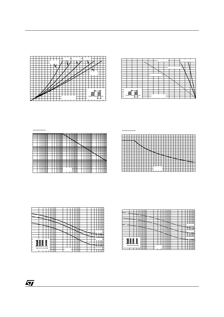
Figure 1: Average forward power dissipation
versus average forward current (per diode)
Figure 2: Average forward current versus
ambient temperature (
= 0.5, per diode)
Figure 3: Normalized avalanche power
derating versus pulse duration
Figure 4: Normalized avalanche power
derating versus junction temperature
Figure 5: Non repetitive surge peak forward
current versus overload duration (maximum
values, per diode)
Figure 6: Non repetitive surge peak forward
current versus overload duration (maximum
values, per diode) (TO-220FPAB)
P
(W)
F(AV)
0
1
2
3
4
5
6
7
8
9
10
0
1
2
3
4
5
6
7
8
9
10
11
12
13
I
(A)
F(AV)
T
=tp/T
tp
= 0.05
= 0.1
= 0.2
= 1
= 0.5
0
1
2
3
4
5
6
7
8
9
10
11
0
25
50
75
100
125
150
175
I
(A)
F(AV)
I≤PAK/TO-220AB
TO-220FPAB
T
(∞C)
amb
T
=tp/T
tp
R
=R
th(j-a)
th(j-c)
R
=15∞C/W
th(j-a)
0.001
0.01
0.1
0.01
1
0.1
10
100
1000
1
t (µs)
p
P
(t )
P
(1µs)
ARM p
ARM
0
0.2
0.4
0.6
0.8
1
1.2
0
25
50
75
100
125
150
T (∞C)
j
P
(t )
P
(25∞C)
ARM p
ARM
I (A)
M
0
20
40
60
80
100
120
140
160
180
1.E-03
1.E-02
1.E-01
1.E+00
T =25∞C
a
T =75∞C
a
T =125∞C
a
I
M
t
=0.5
t(s)
0
10
20
30
40
50
60
70
80
90
100
110
120
1.E-03
1.E-02
1.E-01
1.E+00
I (A)
M
T =25∞C
a
T =75∞C
a
T =125∞C
a
I
M
t
=0.5
t(s)
STPS20S100C
4/7
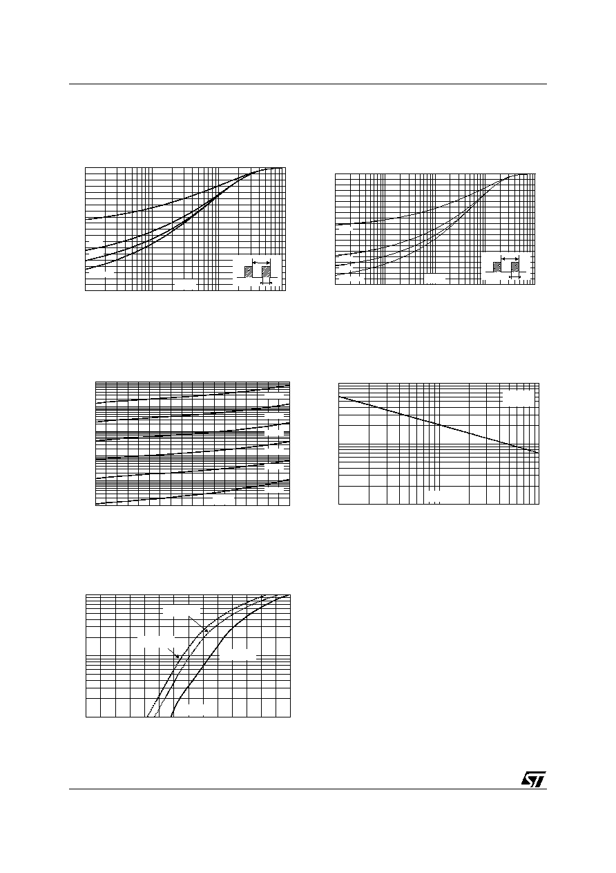
Figure 7: Relative variation of thermal
impedance junction to case versus pulse
duration (per diode)
Figure 8: Relative variation of thermal
impedance junction to case versus pulse
duration (per diode) (TO-220FPAB)
Figure 7: Reverse leakage current versus
reverse voltage applied (typical values, per
diode)
Figure 8: Junction capacitance versus reverse
voltage applied (typical values, per diode)
Figure 9: Forward voltage drop versus forward
current (per diode)
0.0
0.1
0.2
0.3
0.4
0.5
0.6
0.7
0.8
0.9
1.0
1.E-03
1.E-02
1.E-01
1.E+00
Z
/R
th(j-c)
th(j-c)
T
=tp/T
tp
t (s)
p
= 0.5
= 0.2
= 0.1
Single pulse
0.0
0.1
0.2
0.3
0.4
0.5
0.6
0.7
0.8
0.9
1.0
1.E-03
1.E-02
1.E-01
1.E+00
1.E+01
Z
/R
th(j-c)
th(j-c)
T
=tp/T
tp
t (s)
p
= 0.5
= 0.2
= 0.1
Single pulse
I (mA)
R
1.E-04
1.E-03
1.E-02
1.E-01
1.E+00
1.E+01
10
20
30
40
50
60
70
80
90
100
T =125∞C
j
T =150∞C
j
T =100∞C
j
T =50∞C
j
T =25∞C
j
T =75∞C
j
V (V)
R
C(pF)
10
100
1000
1
10
100
V (V)
R
F=1MHz
V
=30mV
T =25∞C
OSC
RMS
j
I
(A)
FM
1
10
100
0.0
0.2
0.4
0.6
0.8
1.0
1.2
1.4
V
(V)
FM
T =25∞C
(maximum values)
j
T =125∞C
(maximum values)
j
T =125∞C
(typical values)
j
STPS20S100C
5/7
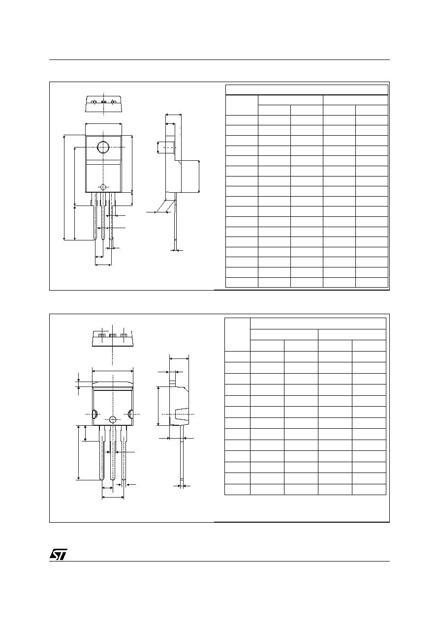
Figure 10: TO-220FPAB Package Mechanical Data
Figure 11: I
2
PAK Package Mechanical Data
H
A
B
Dia
L7
L6
L5
F1
F2
F
D
E
L4
G1
G
L2
L3
E
L2
L1
b1
D
A1
c
c2
A
b
e
e1
L
DIMENSIONS
REF.
Millimeters
Inches
Min.
Max.
Min.
Max.
A
4.4
4.6
0.173
0.181
B
2.5
2.7
0.098
0.106
D
2.5
2.75
0.098
0.108
E
0.45
0.7
0.018
0.027
F
0.75
1
0.03
0.039
F1
1.15
1.7
0.045
0.067
F2
1.15
1.7
0.045
0.067
G
4.95
5.2
0.195
0.205
G1
2.4
2.7
0.094
0.106
H
10
10.4
0.393
0.409
L2
16
Typ.
0.63
Typ.
L3
28.6
30.6
1.126
1.205
L4
9.8
10.6
0.386
0.417
L5
2.9
3.6
0.114
0.142
L6
15.9
16.4
0.626
0.646
L7
9
9.3
0.354
0.366
Dia.
3
3.2
0.118
0.126
REF.
DIMENSIONS
Millimeters
Inches
Min.
Max.
Min.
Max.
A
4.40
4.60
0.173
0.181
A1
2.49
2.69
0.098
0.106
b
0.70
0.93
0.028
0.037
b1
1.14
1.70
0.044
0.067
b2
1.14
1.70
0.044
0.067
c
0.45
0.60
0.018
0.024
c2
1.23
1.36
0.048
0.054
D
8.95
9.35
0.352
0.368
e
2.40
2.70
0.094
0.106
E
10.0
10.4
0.394
0.409
L
13.1
13.6
0.516
0.535
L1
3.48
3.78
0.137
0.149
L2
1.27
1.40
0.050
0.055