Äîêóìåíòàöèÿ è îïèñàíèÿ www.docs.chipfind.ru
®
1/6
Table 1: Main Product Characteristics
I
F(AV)
2 A
V
RRM
150 V
T
j
(max)
175°C
V
F
(max)
0.67 V
STPS2150
POWER SCHOTTKY RECTIFIER
REV. 4
Table 3: Absolute Ratings (limiting values)
Symbol
Parameter
Value
Unit
V
RRM
Repetitive peak reverse voltage
150
V
I
F(RMS)
RMS forward voltage
15
A
I
F(AV)
Average forward current
SMA
T
L
= 145°C
= 0.5
2
A
DO-15
T
L
= 130°C
= 0.5
I
FSM
Surge non repetitive forward
current
SMA
Half wave, single phase,
50Hz
75
A
DO-15
150
P
ARM
Repetitive peak avalanche power
tp = 1µs Tj = 25°C
2400
W
T
stg
Storage temperature range
-65 to + 150
°C
T
j
Maximum operating junction temperature *
175
°C
dV/dt
Critical rate of rise of reverse voltage (rated V
R
, T
j
= 25°C)
10000
V/µs
* :
thermal runaway condition for a diode on its own heatsink
dPt ot
dTj
---------------
1
Rth j
a
(
)
--------------------------
>
SMA
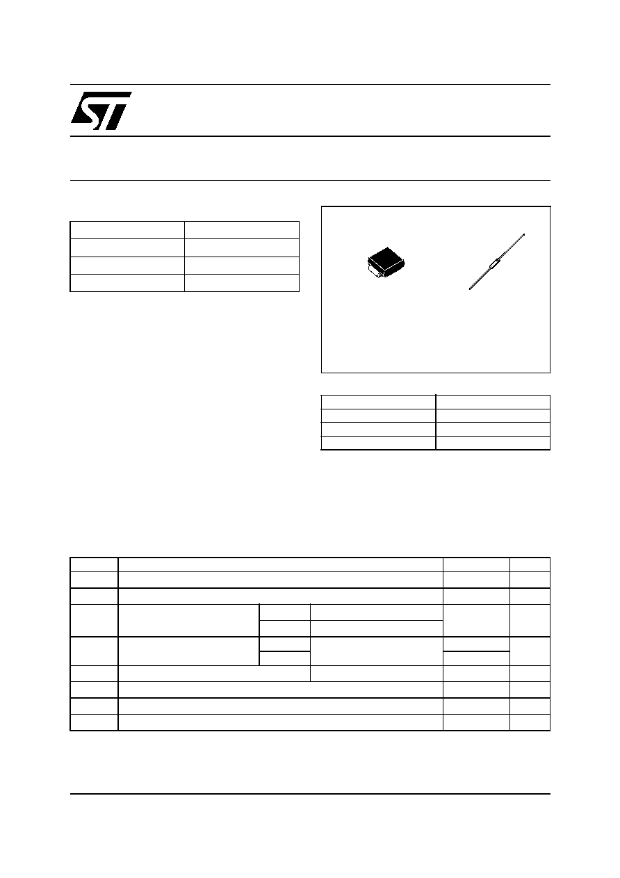
(JEDEC DO-214AC)
STPS2150A
DO-15
STPS2150
August 2004
FEATURES AND BENEFITS
Negligible switching losses
Low forward voltage drop for higher efficiency
and extented battery life
Low thermal resistance
Surface mount miniature package
Avalanche capability specified
DESCRIPTION
150V Power Schottky rectifier are suited for switch
Mode Power Supplies on up to 24V rails and high
frequency converters.
Packaged in SMA and Axial, this device is
intended for use in consumer and computer
applications like TV, STB, PC and DVD where low
drop forward voltage in required to reduce power
dissipation.
Table 2: Order Codes
Part Number
Marking
STPS2150A
2150
STPS2150
STPS2150
STPS2150RL
STPS2150
STPS2150
2/6
Table 4: Thermal Resistance
Table 5: Static Electrical Characteristics
Pulse test:
* tp = 380 µs,
< 2%
To evaluate the conduction losses use the following equation: P = 0.59 x I
F(AV)
+ 0.04 I
F
2
(RMS)
Symbol
Parameter
Value
Unit
R
th(j-l)
Junction to lead
SMA
20
°C/W
Lead length = 10 mm
DO-15
30
Symbol
Parameter
Tests conditions
Min.
Typ
Max.
Unit
I
R
*
Reverse leakage current
T
j
= 25°C
V
R
= V
RRM
0.5
1.5
µA
T
j
= 125°C
0.5
1.5
mA
V
F
*
Forward voltage drop
T
j
= 25°C
I
F
= 2A
0.78
0.82
V
T
j
= 125°C
0.62
0.67
T
j
= 25°C
I
F
= 4A
0.86
0.89
T
j
= 125°C
0.70
0.75
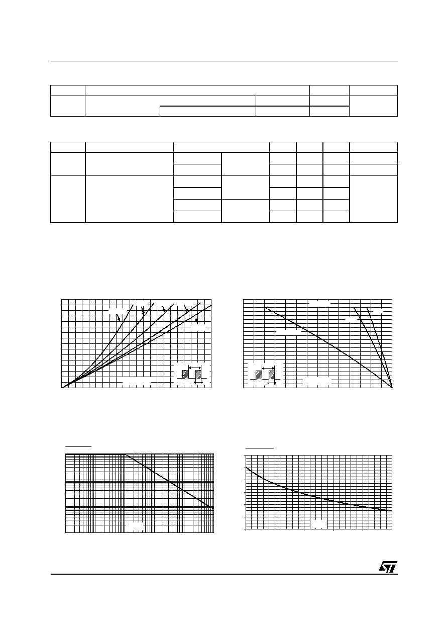
Figure 1: Average forward power dissipation
versus average forward current
Figure 2: Average forward current versus
ambient temperature (
= 0.5)
Figure 3: Normalized avalanche power
derating versus pulse duration
Figure 4: Normalized avalanche power
derating versus junction temperature
P
(W)
F(AV)
0.0
0.2
0.4
0.6
0.8
1.0
1.2
1.4
1.6
0.0
0.2
0.4
0.6
0.8
1.0
1.2
1.4
1.6
1.8
2.0
2.2
I
(A)
F(AV)
T
=tp/T
tp
= 1
= 0.05
= 0.5
= 0.1
= 0.2
I
(A)
F(AV)
0.0
0.2
0.4
0.6
0.8
1.0
1.2
1.4
1.6
1.8
2.0
2.2
0
25
50
75
100
125
150
175
T
=tp/T
tp
T
(°C)
amb
R
=100°C/W
th(j-a)
SMA
DO-15
R
=R
th(j-a)
th(j-I)
0.001
0.01
0.1
0.01
1
0.1
10
100
1000
1
t (µs)
p
P
(t )
P
(1µs)
ARM p
ARM
0
0.2
0.4
0.6
0.8
1
1.2
25
50
75
100
125
150
T (°C)
j
P
(t )
P
(25°C)
ARM p
ARM
STPS2150
3/6
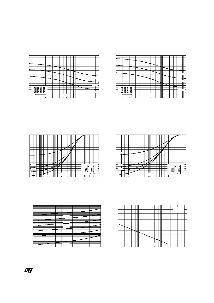
Figure 5: Non repetitive surge peak forward
current versus overload duration (maximum
values) (SMA)
Figure 6: Non repetitive surge peak forward
current versus overload duration (maximum
values) (DO-15)
Figure 7: Relative variation of thermal
impedance junction to ambient versus pulse
duration (epoxy printed circuit board,
e(Cu)=35µm, recommended pad layout) (SMA)
Figure 8: Relative variation of thermal
impedance junction to ambient versus pulse
duration (DO-15)
Figure 9: Reverse leakage current versus
reverse voltage applied (typical values)
Figure 10: Junction capacitance versus
reverse voltage applied (typical values)
I (A)
M
0
1
2
3
4
5
6
7
8
9
10
1.E-03
1.E-02
1.E-01
1.E+00
I
M
t
=0.5
t(s)
T =25°C
a
T =75°C
a
T =125°C
a
I (A)
M
0
1
2
3
4
5
6
7
8
9
10
1.E-03
1.E-02
1.E-01
1.E+00
I
M
t
=0.5
t(s)
T =25°C
a
T =75°C
a
T =125°C
a
Z
/R
th(j-c)
th(j-c)
0.0
0.1
0.2
0.3
0.4
0.5
0.6
0.7
0.8
0.9
1.0
1.E-02
1.E-01
1.E+00
1.E+01
1.E+02
1.E+03
T
=tp/T
tp
t (s)
p
= 0.5
= 0.2
= 0.1
Single pulse
Z
/R
th(j-c)
th(j-c)
0.0
0.1
0.2
0.3
0.4
0.5
0.6
0.7
0.8
0.9
1.0
1.E-01
1.E+00
1.E+01
1.E+02
1.E+03
T
=tp/T
tp
t (s)
p
= 0.5
= 0.2
= 0.1
Single pulse
I (µA)
R
1.E-02
1.E-01
1.E+00
1.E+01
1.E+02
1.E+03
1.E+04
0
25
50
75
100
125
150
T =125°C
j
T =150°C
j
T =100°C
j
T =50°C
j
T =25°C
j
T =75°C
j
V (V)
R
C(nF)
10
100
1000
1
10
100
1000
V (V)
R
F=1MHz
V
=30mV
T =25°C
OSC
RMS
j
STPS2150
4/6
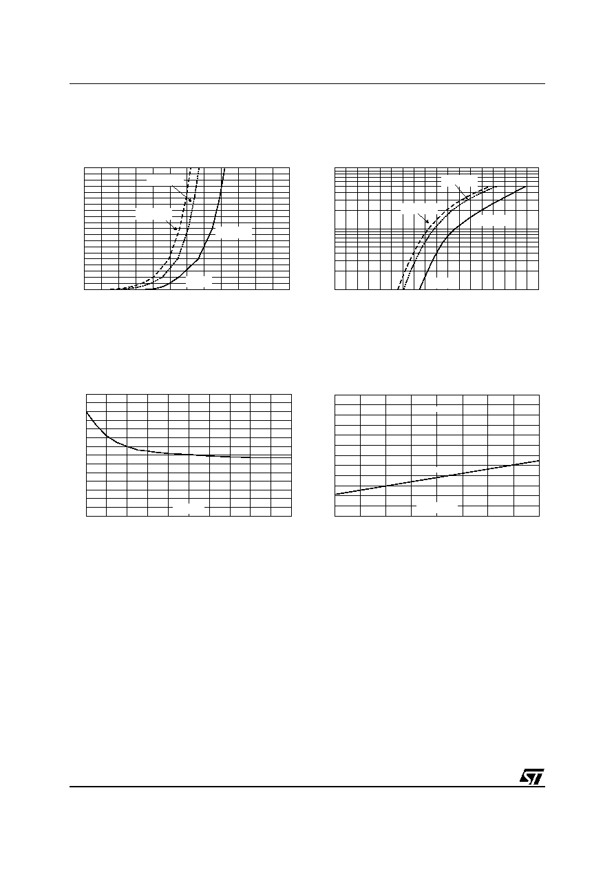
Figure 11: Forward voltage drop versus
forward current (maximum values, high level)
(SMA)
Figure 12: Forward voltage drop versus
forward current (maximum values, low level)
(DO-15)
Figure 13: Thermal resistance junction to
ambient versus copper surface under each
lead (Epoxy printed circuit board FR4, copper
thickness: 35µm) (SMA)
Figure 14: Thermal resistance versus lead
length (DO-15)
I
(A)
FM
0.0
0.2
0.4
0.6
0.8
1.0
1.2
1.4
1.6
1.8
2.0
0.0
0.2
0.4
0.6
0.8
1.0
1.2
T =125°C
(typical values)
j
T =125°C
(maximum values)
j
T =25°C
(maximum values)
j
V
(V)
FM
I
(A)
FM
1
10
100
0.0
0.2
0.4
0.6
0.8
1.0
1.2
1.4
1.6
1.8
V
(V)
FM
T =25°C
(maximum values)
j
T =125°C
(maximum values)
j
T =125°C
(typical values)
j
0
20
40
60
80
100
120
140
0
1
2
3
4
5
R
(°C/W)
th(j-a)
S(cm²)
R (°C/W)
th
0
20
40
60
80
100
120
5
10
15
20
25
R
th(j-a)
R
th(j-I)
L
(mm)
leads
STPS2150
5/6
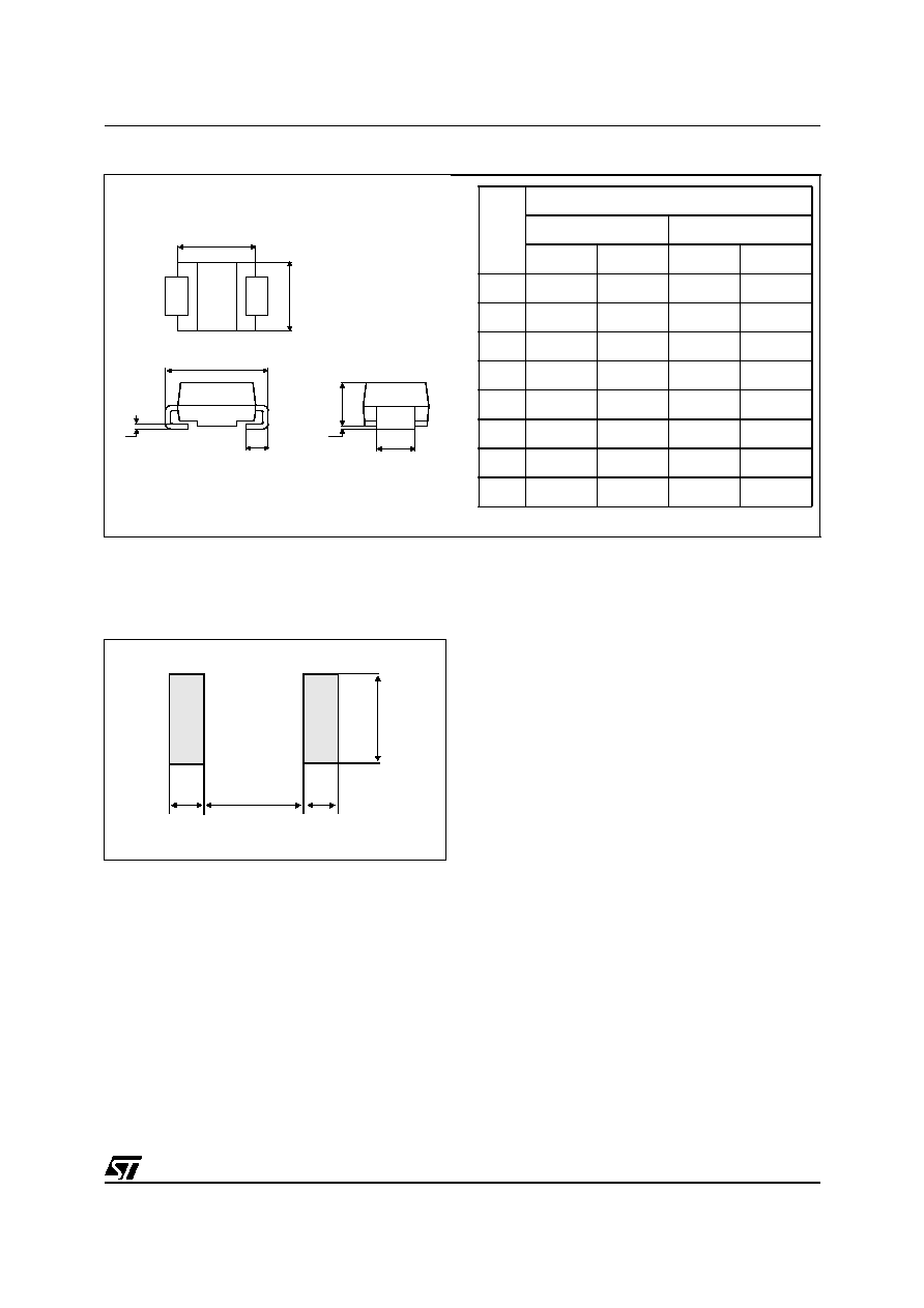
Figure 15: SMA Package Mechanical Data
Figure 16: SMA Foot Print Dimensions
(in millimeters)
E
C
L
E1
D
A1
A2
b
2.40
1.65
1.45
1.45
REF.
DIMENSIONS
Millimeters
Inches
Min.
Max.
Min.
Max.
A1
1.90
2.03
0.075
0.080
A2
0.05
0.20
0.002
0.008
b
1.25
1.65
0.049
0.065
c
0.15
0.41
0.006
0.016
E
4.80
5.60
0.189
0.220
E1
3.95
4.60
0.156
0.181
D
2.25
2.95
0.089
0.116
L
0.75
1.60
0.030
0.063