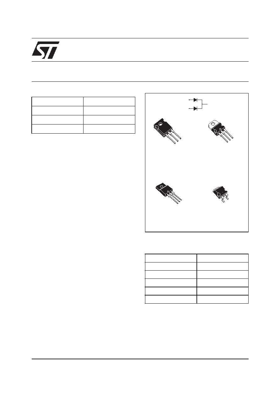
HIGH VOLTAGE POWER SCHOTTKY RECTIFIER
®
1/9
Table 1: Main Product Characteristics
I
F(AV)
2 x 15 A
V
RRM
170 V
T
j
175 °C
V
F
(max)
0.75 V
STPS30170C
HIGH VOLTAGE POWER SCHOTTKY RECTIFIER
REV. 1
K
A1
A2
A1
K
A2
TO-247
STPS30170CW
A1
K
A2
A1
K
A2
A1
K
A2
TO-220AB
STPS30170CT
TO-220FPAB
STPS30170CFP
D
2
PAK
STPS30170CG
September 2005
FEATURES AND BENEFITS
High junction temperature capability
Low leakage current
Good trade off between leakage current and
forward voltage drop
Insulated package: TO-220FPAB
Insulating voltage: 2000 V DC
Capacitance: 45 pF
Avalanche specification
DESCRIPTION
Dual center tab Schottky rectifier suited for High
Frequency Switch Mode Power Supply.
Table 2: Order Codes
Part Numbers
Marking
STPS30170CW
STPS30170CW
STPS30170CT
STPS30170CT
STPS30170CFP
STPS30170CFP
STPS30170CG
STPS30170CG
STPS30170CG-TR
STPS30170CG
STPS30170C
2/9
Table 3: Absolute Ratings (limiting values, per diode)
Table 4: Thermal Parameters
Table 5: Static Electrical Characteristics (per diode)
Pulse test:
* tp = 5 ms,
< 2%
** tp = 380 µs,
< 2%
To evaluate the conduction losses use the following equation: P = 0.64 x IF(AV) + 0.0073 IF
2
(RMS)
Symbol
Parameter
Value
Unit
V
RRM
Repetitive peak reverse voltage
170
V
I
F(RMS)
RMS forward current
30
A
I
F(AV)
Average forward current
= 0.5
TO-220FPAB
Tc = 120 °C
Per diode
Per device
15
A
TO-220AB /
D
2
PAK
Tc = 155 °C
TO-247
30
I
FSM
Surge non repetitive forward current
tp = 10ms sinusoidal
220
A
P
ARM
Repetitive peak avalanche power
tp = 1µs Tj = 25 °C
10500
W
T
stg
Storage temperature range
-65 to + 175
°C
T
j
Maximum operating junction temperature *
175
°C
dV/dt
Critical rate of rise of reverse voltage
10000
V/µs
* :
thermal runaway condition for a diode on its own heatsink
Symbol
Parameter
Value
Unit
R
th(j-c)
Junction to case
TO-220FPAB
Per diode
Total
4
3.3
°C/W
TO-220AB / D
2
PAK
Per diode
Total
1.6
0.85
TO-247
Per diode
Total
1.5
0.8
R
th(c)
TO-220FPAB
Coupling
2.6
°C/W
TO-220AB / D
2
PAK
Coupling
0.3
TO-247
Coupling
0.3
When the diodes 1 and 2 are used simultaneously:
Tj(diode 1) = P(diode 1) x Rth(j-c)(Per diode) + P(diode 2) x Rth(c)
Symbol
Parameter
Tests conditions
Min.
Typ
Max.
Unit
I
R
*
Reverse leakage current
T
j
= 25 °C
V
R
= V
RRM
20
µA
T
j
= 125 °C
5
20
mA
V
F
**
Forward voltage drop
T
j
= 25 °C
I
F
= 15 A
0.92
V
T
j
= 125 °C
0.69
0.75
T
j
= 25 °C
I
F
= 30 A
1
T
j
= 125 °C
0.80
0.86
dPtot
dTj
---------------
1
Rth j
a
(
)
--------------------------
>
STPS30170C
3/9
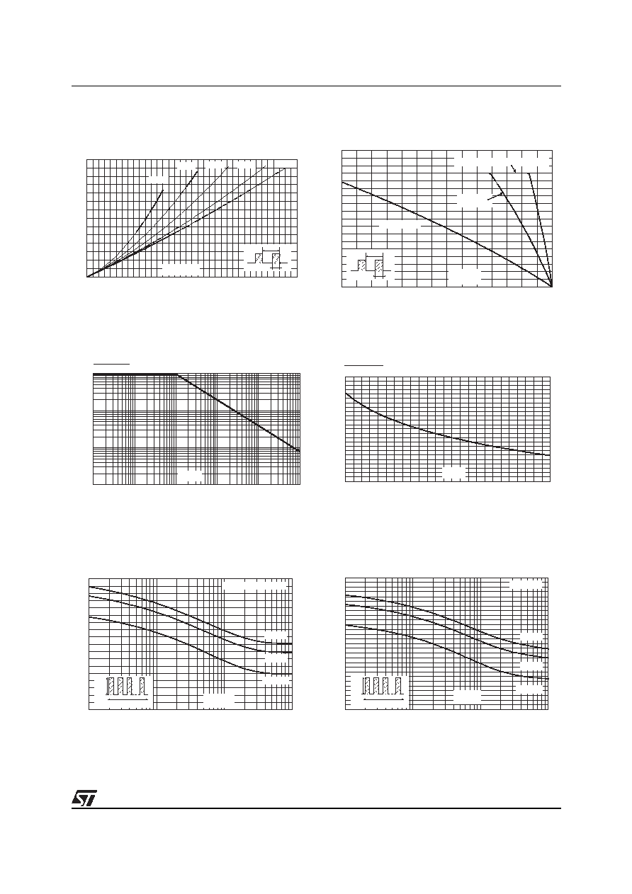
Figure 1: Average forward power dissipation
versus average forward current (per diode)
Figure 2: Average forward current versus
ambient temperature (
= 0.5, per diode)
Figure 3: Normalized avalanche power
derating versus pulse duration
Figure 4: Normalized avalanche power
derating versus junction temperature
Figure 5: Non repetitive surge peak forward
current versus overload duration (maximum
values, per diode) (TO-220AB, TO-247, D
2
PAK)
Figure 6: Non repetitive surge peak forward
current versus overload duration (maximum
values, per diode) (TO-220FPAB)
0
2
4
6
8
10
12
14
0
1
2
3
4
5
6
7
8
9
10 11 12 13 14 15 16 17 18
P
F(AV)
(W)
d=0.05
d=0.1
d=0.2
d=0.5
d=1
T
d
=t /T
p
t
p
I
F(AV)
(A)
0
2
4
6
8
10
12
14
16
18
0
25
50
75
100
125
150
175
I
F(AV)
(A)
R
th
(j-A)
=15 °C/W
T
d
=t /T
p
t
p
R
th(j-a)
=R
th(j-c)
(TO-220AB, TO -247 & D²PAK)
R
th(j-a)
=R
th(j-c)
(TO-220AB, TO -247 & D²PAK)
R
th(j-a)
=R
th(j-c)
(TO-220FPAB)
R
th(j-a)
=R
th(j-c)
(TO-220FPAB)
T
amb
(°C)
0.001
0.01
0.1
0.01
1
0.1
10
100
1000
1
t (µs)
p
P
(t )
P
(1µs)
ARM p
ARM
0
0.2
0.4
0.6
0.8
1
1.2
25
50
75
100
125
150
T (°C)
j
P
(t )
P
(25°C)
ARM p
ARM
0
25
50
75
100
125
150
175
200
225
1.E-03
1.E-02
1.E-01
1.E+00
I
M
(A)
T
C
=50°C
T
C
=75°C
T
C
=125°C
I
M
t
d
=0.5
TO-220AB, TO -247 & D²PAK
t(s)
0
10
20
30
40
50
60
70
80
90
100
110
120
130
140
1.E-03
1.E-02
1.E-01
1.E+00
I
M
(A)
T
C
=50°C
T
C
=75°C
T
C
=125°C
I
M
t
d
=0.5
TO-220FPAB
t(s)
STPS30170C
4/9
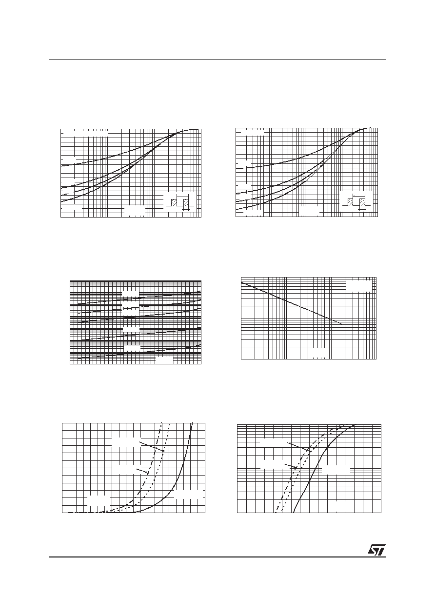
Figure 7: Relative variation of thermal
impedance junction to case versus pulse
duration (per diode) (TO-220AB, TO-247,
D
2
PAK)
Figure 8: Relative variation of thermal
impedance junction to case versus pulse
duration (per diode) (TO-220FPAB)
Figure 9: Reverse leakage current versus
reverse voltage applied (typical values, per
diode)
Figure 10: Junction capacitance versus
reverse voltage applied (typical values, per
diode)
Figure 11: Forward voltage drop versus
forward current (maximum values, per diode,
low level)
Figure 12: Forward voltage drop versus
forward current (maximum values, per diode,
high level)
0.0
0.1
0.2
0.3
0.4
0.5
0.6
0.7
0.8
0.9
1.0
1.E-03
1.E-02
1.E-01
1.E+00
Z
th(j-c)
/R
th(j-c)
d=0.1
d=0.2
d=0.5
Single pulse
T
d
=t /T
p
t
p
TO-220AB, TO -247 & D²PAK
t
P
(s)
0.0
0.1
0.2
0.3
0.4
0.5
0.6
0.7
0.8
0.9
1.0
1.E-03
1.E-02
1.E-01
1.E+00
1.E+01
Z
th(j-c)
/R
th(j-c)
D=0.1
d=0.2
d=0.5
Single pulse
T
d
=t /T
p
t
p
TO-220FPAB
t
P
(s)
1.E-01
1.E+00
1.E+01
1.E+02
1.E+03
1.E+04
1.E+05
1.E+06
0
10 20 30 40 50 60 70 80 90 100 110 120 130 140 150 160 170
I
R
(µA)
T
j
=150°C
T
j
=125°C
T
j
=25°C
T
j
=75°C
T
j
=175°C
V
R
(V)
10
100
1000
1
10
100
1000
C(pF)
F=1MHz
V
OSC
=30mV
RMS
T
j
=25°C
V
R
(V)
I
FM
(A)
0.0
2.5
5.0
7.5
10.0
12.5
15.0
0.0
0.1
0.2
0.3
0.4
0.5
0.6
0.7
0.8
0.9
1.0
Tj=25°C
(Maximum values)
Tj=125°C
(Maximum values)
Tj=125°C
(Maximum values)
Tj=125°C
(Typical values)
Tj=125°C
(Typical values)
V
FM
(V)
I
FM
(A)
1
10
100
0.0
0.2
0.4
0.6
0.8
1.0
1.2
1.4
1.6
Tj=25°C
(Maximum values)
Tj=125°C
(Maximum values)
Tj=125°C
(Maximum values)
Tj=125°C
(Typical values)
Tj=125°C
(Typical values)
V
FM
(V)
STPS30170C
5/9
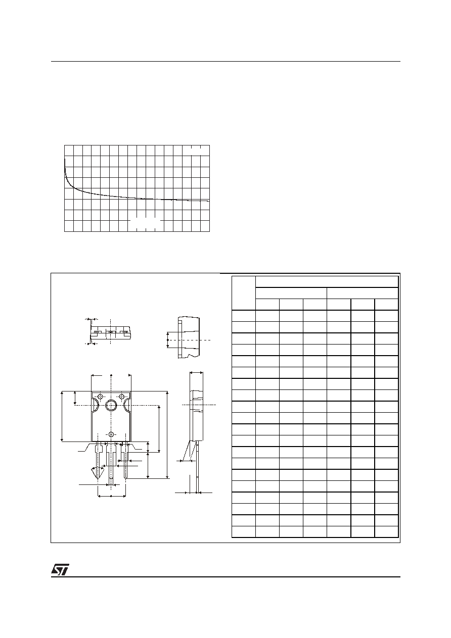
Figure 14: TO-247 Package Mechanical Data
Figure 13: Thermal resistance junction to
ambient versus copper surface under tab
(Epoxy printed circuit board, copper
thickness: 35 µm) (D
2
PAK)
0
10
20
30
40
50
60
70
80
0
5
10
15
20
25
30
35
40
R
th(j-a)
(°C/W)
D²PAK
S
CU
(cm²)
H
L2
L5
L
L4
D
E
M
L1
L3
F2
F3
F4
F1
V2
F(x3)
G
A
V
V
Dia
REF.
DIMENSIONS
Millimeters
Inches
Min.
Typ.
Max.
Min.
Typ.
Max.
A
4.85
5.15
0.191
0.203
D
2.20
2.60
0.086
0.102
E
0.40
0.80
0.015
0.031
F
1.00
1.40
0.039
0.055
F1
3.00
0.118
F2
2.00
0.078
F3
2.00
2.40
0.078
0.094
F4
3.00
3.40
0.118
0.133
G
10.90
0.429
H
15.45
15.75 0.608
0.620
L
19.85
20.15 0.781
0.793
L1
3.70
4.30
0.145
0.169
L2
18.50
0.728
L3
14.20
14.80 0.559
0.582
L4
34.60
1.362
L5
5.50
0.216
M
2.00
3.00
0.078
0.118
V
5°
5°
V2
60°
60°
Dia.
3.55
3.65
0.139
0.143